Self-oscillation type switching power supply having time constant circuit electronic switch an external voltage and having charging time variable in response to output voltage

a self-oscillation switching and power supply technology, applied in the direction of power conversion systems, dc-dc conversion, instruments, etc., can solve the problems of delay in the supply of base current, inability to achieve stable control, and difficulty in achieving oscillation at a frequency higher than the intrinsic resonance frequency

Inactive Publication Date: 2000-03-14
MURATA MFG CO LTD
View PDF4 Cites 43 Cited by
  • Summary
  • Abstract
  • Description
  • Claims
  • Application Information

AI Technical Summary

Problems solved by technology

In the conventional self-oscillation switching power supply shown in FIG. 16, a step-down transformer is employed as the transformer T, and the output voltage Vout is limited to a rather low voltage such as 5 V. Using the circuit configuration shown in FIG. 16, it is possible to produce a power supply capable of generating a high voltage by increasing the ratio of the number of turns of the secondary windings Ls to that of the primary winding Lp of the transformer T. However, such a power supply will have the following problems.
In contrast, the high-voltage transformer has a very low intrinsic resonance frequency fo, as described above, and therefore, it is difficult to achieve oscillation at a frequency higher than the intrinsic resonance frequency even when there is no load which consumes the output power.
As a result, a delay occurs in the supply of the base current from the positive feedback winding Lf to the switching transistor Q1.
Therefore, it is impossible to achieve stable control and the output voltage includes large ripples.
Leakage inductance of the transformer is another problem which occurs when the low-voltage transformer T shown in FIG. 16 is replaced with the high-voltage transformer shown in FIG. 17. FIG. 19 illustrates an equivalent circuit of the high-voltage transformer and the switching transistor.
This causes an unstable circuit operation such as intermittent oscillation.
Furthermore, because the switching transistor Q1 turns on and off at a high frequency, the switching loss increases and thus it becomes necessary to employ a larger-size heat sink.
This ringing component superimposed on the collector current Ic adversely affects the control operation of the circuit based on the technique in which the output is stabilized by controlling the on-period of the switching transistor Q1.
Because this maximum value of the on-period is much greater than the rated value in the normal state, an initial voltage corresponding to the maximum on-period is induced across the secondary winding Ls and thus a great overshoot occurs.
Thus, the circuit becomes complicated in configuration and large in size.
However, the impedance circuit prevents the control transistor or the delay transistor from being reverse-biased, and thus the control transistor or the delay transistor turns off after a short delay due to the effect of carrier accumulation in the transistor.

Method used


Image

  • Self-oscillation type switching power supply having time constant circuit electronic switch an external voltage and having charging time variable in response to output voltage
  • Self-oscillation type switching power supply having time constant circuit electronic switch an external voltage and having charging time variable in response to output voltage
  • Self-oscillation type switching power supply having time constant circuit electronic switch an external voltage and having charging time variable in response to output voltage

Examples


first embodiment

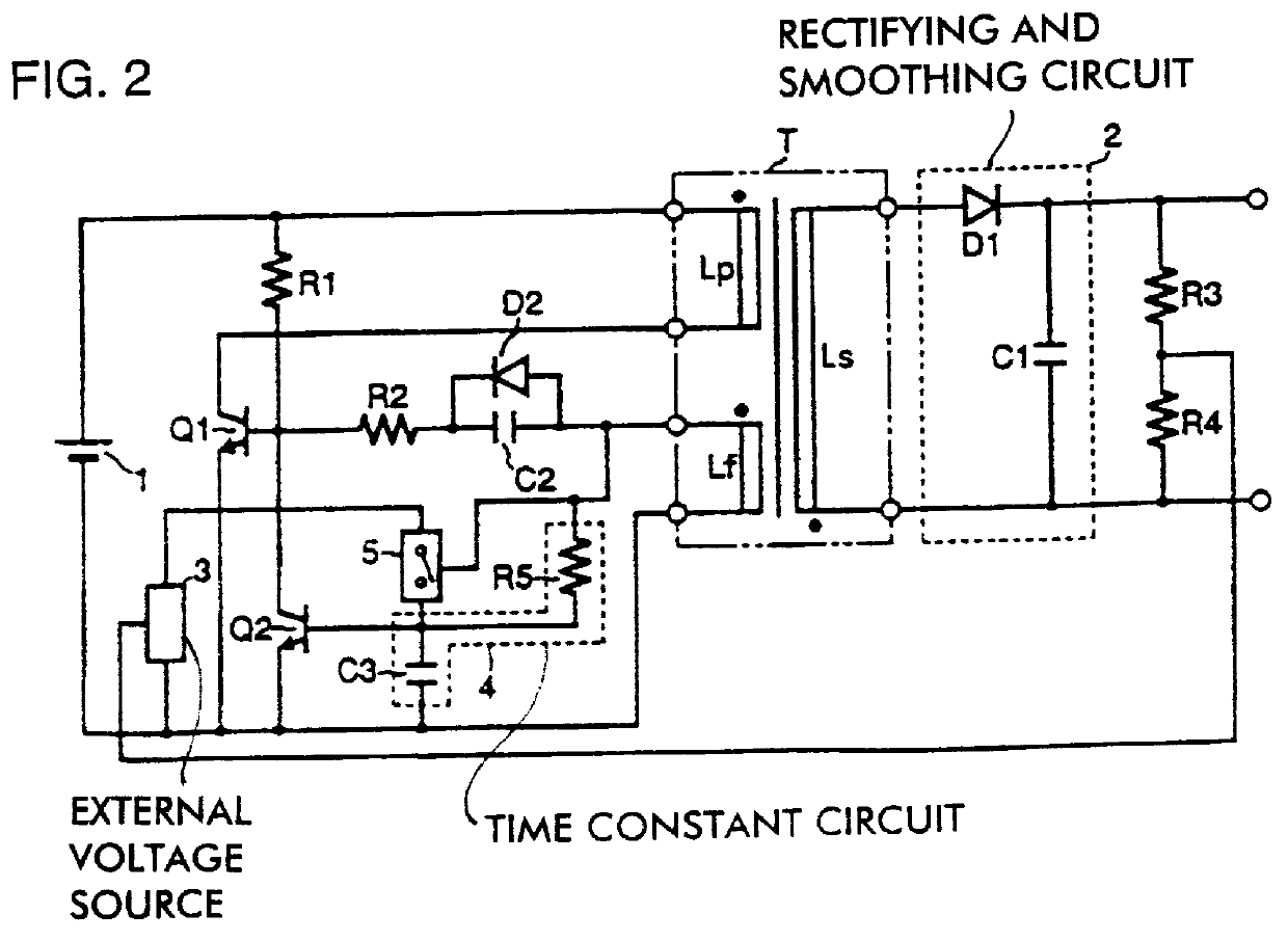
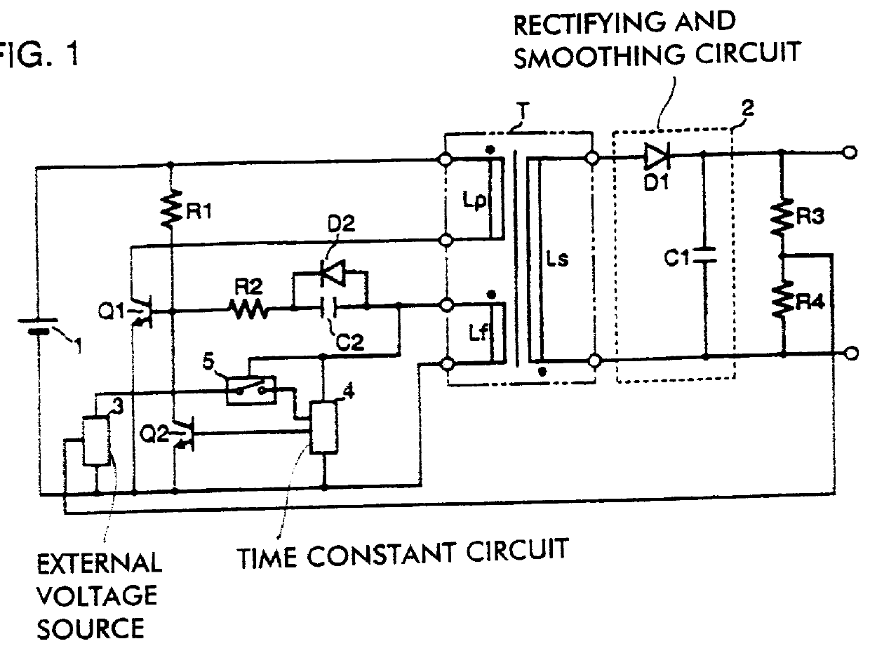
FIG. 1 is a circuit diagram illustrating a general example of a circuit configuration of the self-oscillation switching power supply according to the present invention. In FIG. 1, reference numeral 1 denotes an input power supply, T denotes a high-voltage transformer including a primary winding Lp, a secondary winding Ls, and a feedback winding Lf. Q1 denotes the switching transistor connected to the input power supply via the primary winding Lp of the high-voltage transformer T. A starting resistor R1 is connected to the base of the switching transistor Q1. A current limiting resistor R2, a speed-up capacitor C2, and a diode D2 are disposed between the feedback winding Lf and the base of the switching transistor Q1. The control transistor Q2 is connected between the base and the emitter of the switching transistor Q1. The feedback winding Lf is connected to a time constant circuit 4 so that a voltage generated by the time constant circuit 4 is applied to the base of the control tra...

second embodiment

FIG. 4 is a circuit diagram illustrating a self-oscillation switching power supply. The difference from the circuit shown in FIG. 3 is that there is provided an additional diode D5 between the capacitor C3 of the time constant circuit and the base of the control transistor Q2. Although not shown in FIG. 4, the switching power supply also includes a remote control circuit. The diode D5 additionally disposed in the circuit serves to cut off a reverse bias current which would otherwise flow into the control transistor Q2 from the feedback winding Lf when the switching transistor Q1 turns off. As a result, high-frequency response is prevented by the carrier accumulation effect in the control transistor Q2. This limits the maximum oscillation frequency of the switching transistor Q1. As a result, the high-frequency oscillation at the series resonance frequency associated with the circuit formed by the leakage inductance and the distributed capacitance of the high-voltage transformer is s...

third embodiment

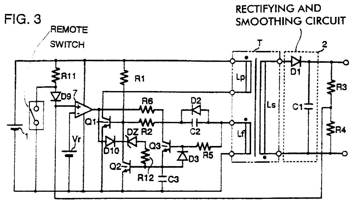
FIG. 5 is a circuit diagram illustrating a self-oscillation switching power supply. The difference from the circuit shown in FIG. 3 is that there is provided a delay transistor Q4 between the base and the emitter of the switching transistor Q1 and there are also provided a control winding Lc and an impedance circuit 8 so that a control signal is generated by the control winding Lc and applied to the delay transistor Q4 via the impedance circuit 8. The polarity of the voltage induced across the control winding Lc is opposite to that of the feedback winding Lf. More specifically, a positive voltage is induced during the off-period of the switching transistor Q1 whereby the delay transistor Q4 is forward-biased between its base and emitter, via the impedance circuit including the current limiting resistor R7 and the diode D4. After that, a voltage is induced across the feedback winding by the resonant oscillation of the high-voltage transformer T whereby the base of the switching trans...


PUM


Abstract

A self-oscillation switching power supply including a transformer having a primary winding, a secondary winding, and a feedback winding, and further including a control winding if necessary; a switching transistor for turning on and off the current of the primary winding; a control transistor for controlling a positive feedback signal from the feedback winding or control winding to the switching transistor; and a time constant circuit which is charged by a voltage generated across the feedback winding or control winding and which supplies a control voltage to the control transistor. The self-oscillation switching power supply further comprises an electronic switch which is opened and closed in response to the positive feedback signal from the control winding or feedback winding wherein an external voltage source is connected to the time constant circuit via said electronic switch so that the charging time of the time constant circuit is varied according to an output voltage detection signal.

Description

1. Field of the InventionThe present invention relates to a self-oscillation switching power supply, and more particularly, to a switching power supply for outputting a high voltage.2. Description of the Related ArtA ringing choke converter is widely used as a self-oscillation switching power supply. FIG. 16 is a circuit diagram of a ringing choke converter according to a conventional technique. In FIG. 16, reference numeral 11 denotes a DC power supply circuit which generates a DC voltage of about 120 V by rectifying and smoothing commercial AC electric power. T denotes a transformer with a primary winding Lp, a secondary winding Ls, and a feedback winding Lf. Q1 denotes a switching transistor connected to the DC power supply via the primary winding Lp of the transformer T. The base of the switching transistor Q1 is connected to a starting resistor R1. The base of the transistor Q1 is also connected to the feedback winding Lf via a current limiting resistor R2, a speed-up capacitor...

Claims


Application Information

Patent Timeline
Patent Type & Authority Patents(United States)
IPC IPC(8): H02M3/24H02M3/338H02M3/28
CPCH02M3/3385
Inventor MIYAZAKI, KENGOIJIRI, YASUNORI
Owner MURATA MFG CO LTD
Why Eureka
Try Eureka