Semiconductor light-emitting device

Inactive Publication Date: 2000-03-21
TOYODA GOSEI CO LTD
View PDF3 Cites 118 Cited by
  • Summary
  • Abstract
  • Description
  • Claims
  • Application Information

AI Technical Summary

Problems solved by technology

This is because there is a danger that the wavelengths of light emitted from the respective quantum well layers will be slightly varied by the quantum effect if thicknesses differ between layers.
Therefore, there is a danger that the wavelengths of light will be shifted.
Further, if a clad layer is of the n-type and a quantum well layer is contiguous to such clad layer, the well is hard to form in such quantum we

Method used


Image

  • Semiconductor light-emitting device
  • Semiconductor light-emitting device
  • Semiconductor light-emitting device

Examples


first embodiment

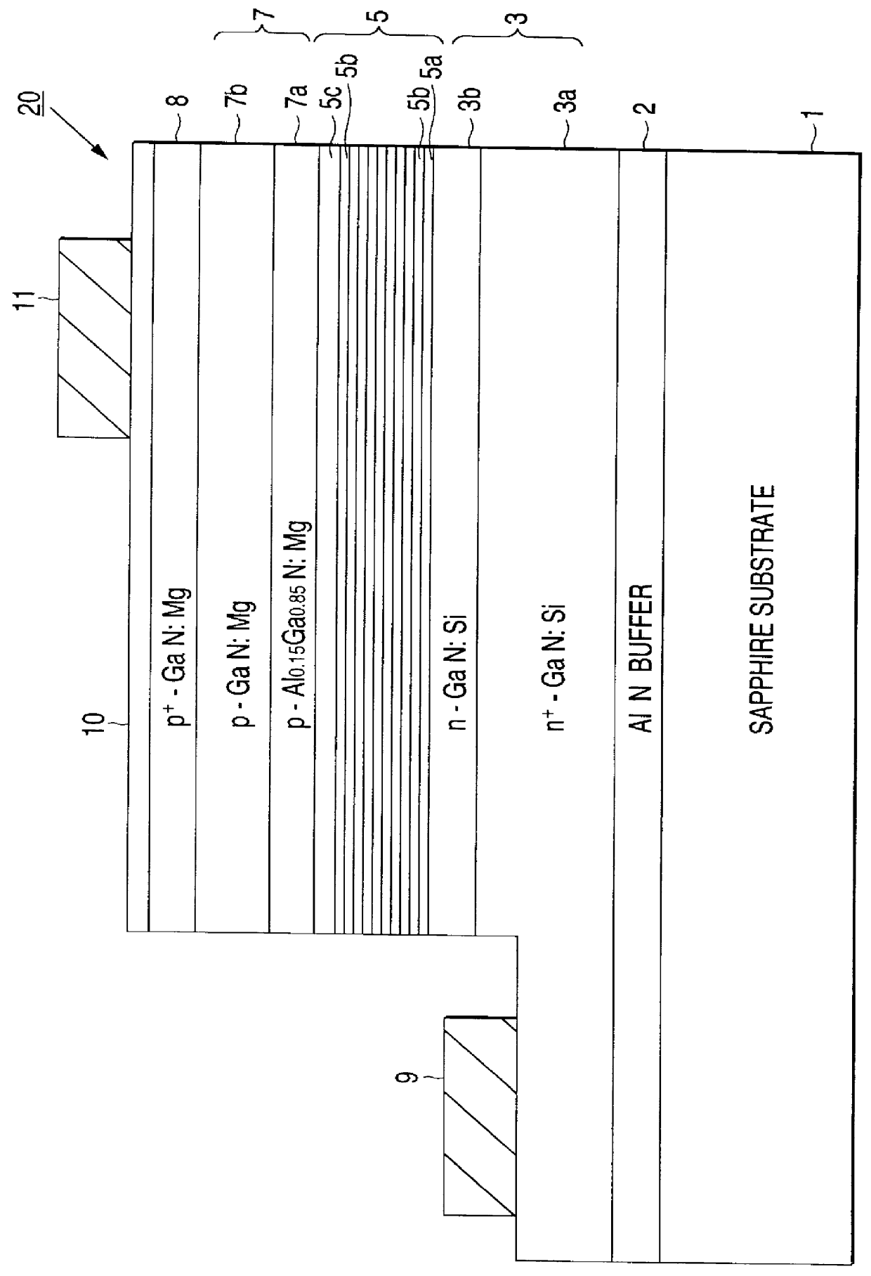
A semiconductor light-emitting device according to this embodiment is a blue light-emitting diode. FIG. 1 is a sectional view of a light-emitting diode 20, which is the first embodiment.

A 20 nm-thick buffer layer 2 made of AlN is formed on a plane a of a 100 .mu.m-thick sapphire substrate 1. The thickness of the buffer layer 2 may be set to 20 to 50 nm, and the film is grown at 400.degree. C.

An n-type semiconductor layer 3 is formed on the buffer layer 2 in two layers. The n layer 3 includes: a 2.5 .mu.m-thick n.sup.+ -GaN layer 3a with silicon doped at high density (carrier concentration is 2.times.10.sup.18 / cm.sup.3); and a 0.5 .mu.m-thick silicon-doped n-GaN layer 3b (a first clad-layer (a first semiconductor layer), carrier concentration: 2.times.10.sup.17 / cm.sup.3).

The n layer 3 may be formed of a compound semiconductor made of Al.sub.X In.sub.Y Ga.sub.1-X-Y N (including X=0, X=Y, X=Y=0). The n layer 3 may also be designed as a single layer.

A light-emitting layer 5 of superla...

second embodiment

A semiconductor light-emitting device according to this embodiment is a green light-emitting diode.

The light-emitting diode according to this embodiment is distinguished from the light-emitting diode according to the first embodiment in that the quantum well layers have a composition of In.sub.0.23 Ga.sub.0.77 N. That is, the indium mole fraction of the quantum well layers is increased compared with that in the first embodiment. Such quantum well layers are formed by increasing the flow rate of TMI or the like similarly to the first embodiment.

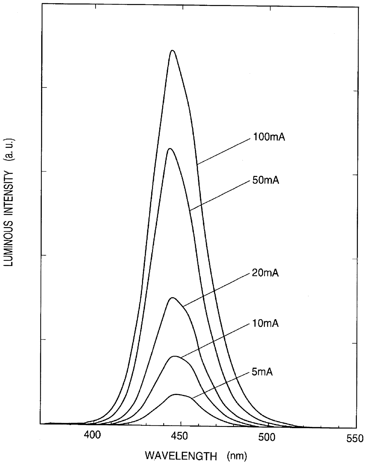
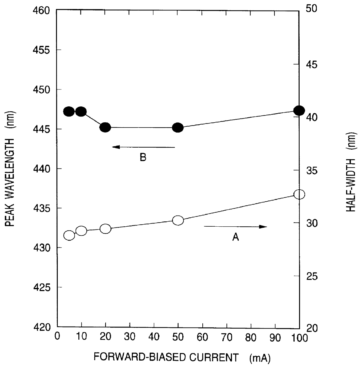
According to an examination carried out by the inventors, the following characteristics are exhibited by the thus formed device according to the second embodiment.

FIG. 4 shows emission spectral changes observed when forward-biased current applied to the device is varied. FIG. 5 is an analysis of the emission spectra of FIG. 4, and shows changes in peak wavelength and half-width observed when forward-biased current applied to the device is vari...


PUM


Abstract

A semiconductor light-emitting device involving the steps of: forming a first semiconductor layer; forming a light-emitting layer of superlattice structure by laminating a barrier layer being made of InY1Ga1-Y1N (Y1>/=0) and a quantum well layer being made of InY2Ga1-Y1N (Y2>Y1 and Y2>0) on the first semiconductor layer; and forming a second semiconductor layer on the light-emitting layer, an uppermost barrier layer, which will become an uppermost layer of the light-emitting layer, is made thicker than the other barrier layers. Further, at the time of forming the second semiconductor layer, an upper surface of such uppermost barrier layer is caused to disappear so that the thickness of the uppermost barrier layer becomes substantially equal to those of the other barrier layers.

Description

1. Field of the InventionThe invention relates to a semiconductor light-emitting device and a method of manufacturing said semiconductor light-emitting device. The semiconductor light-emitting device can be utilized as, e.g., a light-emitting diode and a laser diode.2. Description of the Related ArtLight-emitting devices using compound semiconductors are known as those covering visible to short wavelength regions. Among others, group III nitride semiconductors have attracted attention in recent years, not only because these semiconductors are of direct transition type, so that they exhibit high light-emitting efficiency, but also because these semiconductors emit blue light, which is one of the three primary colors.One example of such light-emitting device is formed by laminating an AlN buffer layer, a first clad layer, a light-emitting layer, and a second clad layer sequentially on a sapphire substrate. Here, the first and the second clad layers are made of Al.sub.X In.sub.Y Ga.sub...

Claims


Application Information

Patent Timeline
IPC IPC(8): H01L33/00H01L29/02H01L29/15H01L33/06H01L33/32H01L33/40H01S5/00H01S5/323H01S5/343
CPCB82Y20/00H01L29/155H01L33/06H01L33/32Y10S438/933H01L33/00
Inventor KOIDE, NORIKATSUASAMI, SHINYAUMEZAKI, JUNICHIKOIKE, MASAYOSHIYAMASAKI, SHIRONAGAI, SEIJI
Owner TOYODA GOSEI CO LTD
Why Eureka
Try Eureka