Waveguide pair with cladding

a waveguide and cladding technology, applied in the field of dielectric waveguide pairs, can solve problems such as loss

Inactive Publication Date: 2000-03-28
NORTEL NETWORKS UK +1
View PDF13 Cites 47 Cited by
  • Summary
  • Abstract
  • Description
  • Claims
  • Application Information

AI Technical Summary

Problems solved by technology

Such losses can arise from irregularities o

Method used


Image

  • Waveguide pair with cladding

Examples


Embodiment Construction

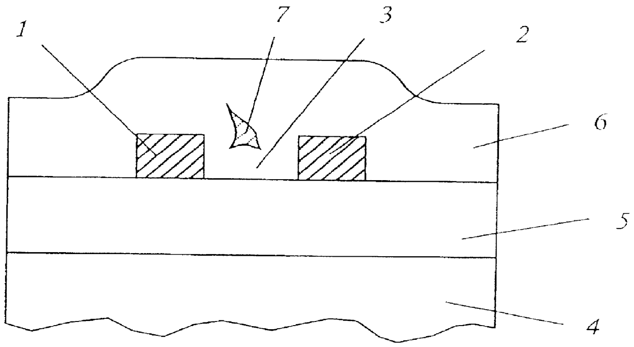
Referring to the drawing, a dielectric waveguide pair produced by PECVD on a planar substrate seen in cross-section is assumed to extend an appreciable distance into and out of the plane of the drawing, for transmitting the optical energy longitudinally and for coupling some energy across to the intervening medium. The coupling devices may be a Y-junction, a directional coupler or a radiative star and the like, where parallel lengths of waveguide are as close as less than one micron (1 .mu.m) to each other. The figure shows two waveguide cores 1, 2 which have been deposited on a substrate 4, suitably of silicon, with an intervening buffer layer 5. Buffer layer 5, which is preferably of silica inhibits the optical fields arising during operation from interacting with substrate 4. The cores and the buffer, at least in surrounding regions, are covered with a layer of cladding 6 which may be 20 .mu.m or more thick, and which plays protective and optical roles.

If the heights of the waveg...


PUM

PropertyMeasurementUnit
Percent by massaaaaaaaaaa
Angleaaaaaaaaaa

Abstract

PCT No. PCT/GB97/00040 Sec. 371 Date Apr. 12, 1999 Sec. 102(e) Date Apr. 12, 1999 PCT Filed Jan. 8, 1997 PCT Pub. No. WO97/25636 PCT Pub. Date Jul. 17, 1997A planar waveguide structure has, supported on a lower refractive index buffer layer (5), a pair of optical cores (1, 2) that, over at least a portion of their length, are closely spaced. These cores are covered with a layer (6) of cladding material comprising boron and phosphorus doped silica glass deposited by PECVD as a succession of individually annealed layers in order to minimize the incidence of voids in the deposit between the cores.

Description

BACKGROUND TO THE INVENTIONThe present invention relates to dielectric waveguide pairs made by plasma enhanced chemical vapour deposition (PECVD) upon planar substrates. Such deposition involves depositing and patterning material to form cores of material having a slightly greater refractive index than that of buffer layer material upon which those cores are supported and that of cladding material with which those cores are covered. Typically these waveguide pairs are designed for guiding light in the 1 to 2 .mu.m for optical communication systems.The invention is particularly concerned with waveguide pairs in which their waveguide cores approach close enough together to provide a significant amount of cross coupling either from the cores, or between the cores, without undue losses. Such losses can arise from irregularities or discontinuities in the intervening medium.Embodiments of the invention aim to provide cladding for the cores produced by PECVD which maintain good and low-los...

Claims


Application Information

Patent Timeline
IPC IPC(8): G02B6/125G02B6/132G02B6/13G02B6/12G02B6/122
CPCG02B6/125G02B6/13G02B6/132G02B2006/12147G02B2006/12169
Inventor GRANT, MICHAEL FRANCISDAY, STEPHEN
Owner NORTEL NETWORKS UK
Why Eureka
Try Eureka