Display device and method of manufacturing the same
a technology of display device and manufacturing method, which is applied in the manufacture of electrode systems, electric discharge tubes/lamps, instruments, etc., can solve the problems of prone to cracking, thin, short and small, and lightness of portable electronic instruments, and achieve the effect of thin glass substrates, thinned glass substrates, and easy cracking
- Summary
- Abstract
- Description
- Claims
- Application Information
AI Technical Summary
Problems solved by technology
Method used
Image
Examples
example 2
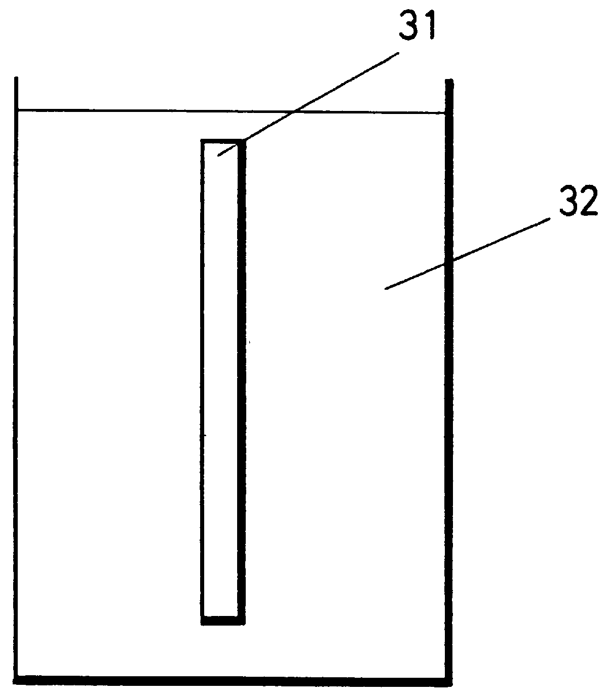
A display device was manufactured as in Example 1 except that the strengthening solution in FIG. 3 (c) of the Example 1 is composed of a mixed molten salt of 50% KNO.sub.3 and 50% RbNO.sub.3 with an effect similar to that of Example 1.
example 3
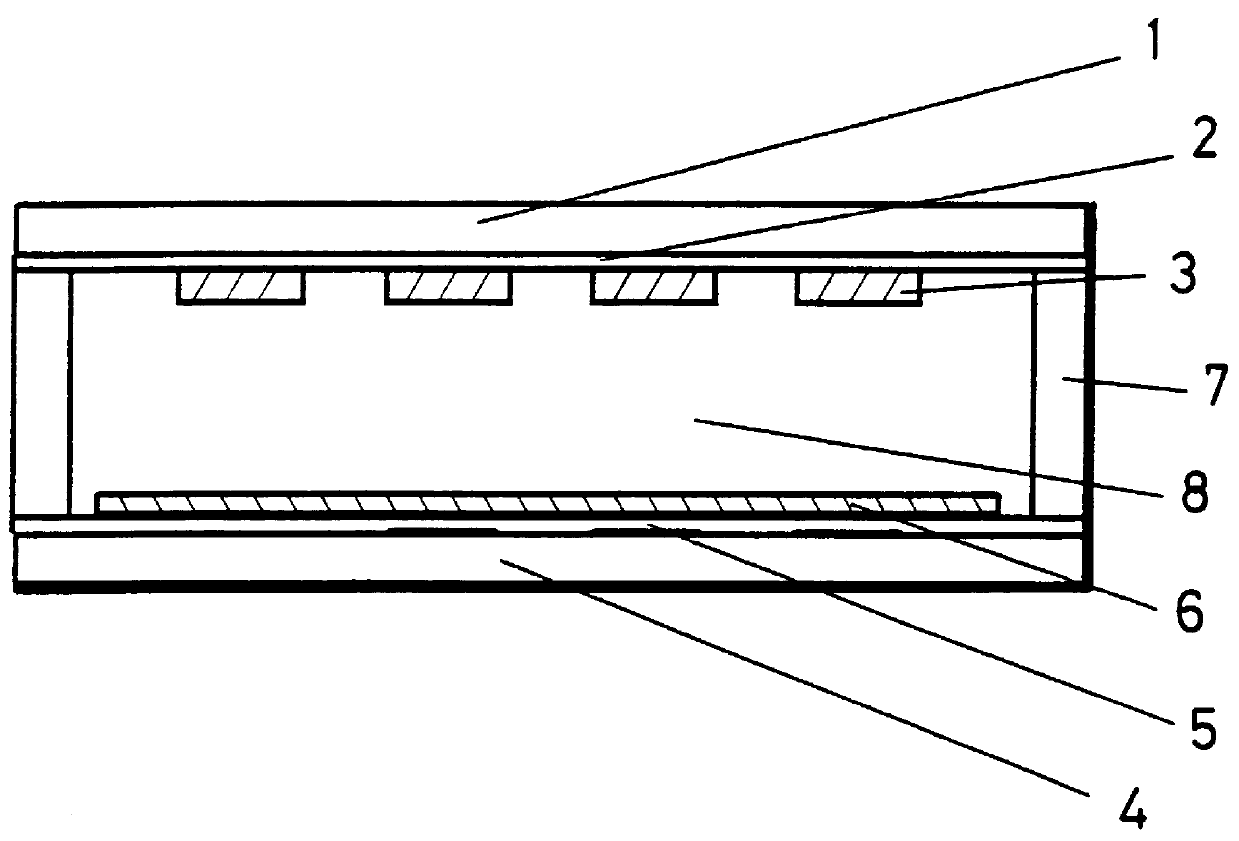
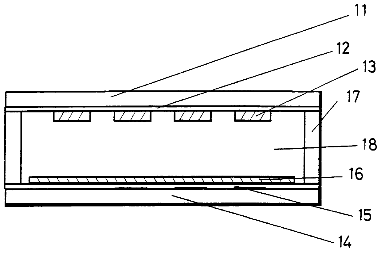
In FIG. 1 a sodium passivation film 2 made of SiO.sub.2 is formed on a glass substrate 1 made of soda glass having a thickness of 0.55 mm of which surface has been polished and a film of ITO is successively formed and patterned by a method such as vapor deposition, sputtering or the like thereby forming a transparent electrode 3. Similarly, a sodium passivation film 5 and a transparent electrode 6 are successively laminated on a polished glass substrate 4, the glass substrate 1 and the glass substrate 4 are opposed to each other and both are pasted together by a sealing agent 7 thereby forming a display cell.
Next, a chemical strengthening is carried out by a method illustrated by FIG. 4.
In FIG. 4 (a) the above-mentioned display cell 41 is prepared. One thing to be careful about here is a necessity of sealing holes such as liquid crystal injection ports, provided on the display cell such that a solution does not enter the holes. In FIG. 4 (b) the display cell 41 is chemically strengt...
example 4
In FIG. 1 a sodium passivation film 2 made of SiO.sub.2 is formed on a glass substrate 1 made of soda glass having a thickness of 0.55 mm of which surface has been polished and a film of ITO is formed and patterned by a method such as vapor deposition, sputtering or the like thereby forming a transparent electrode 3. Similarly a sodium passivation film 5 and a transparent electrode 6 are successively laminated on a polished glass substrate 4, the glass substrate 1 and the glass substrate 4 are opposed to each other, both are pasted together by a sealing agent 7 and a display material 8 composed of liquid crystals is filled in the clearance thereby forming a display device.
Next, a chemical strengthening is performed by a method illustrated by FIG. 4.
In FIG. 4 (a) the above-mentioned display device 41 is prepared. In FIG. 4 (b) the display cell 41 is chemically strengthened at 100.degree. C. by dipping it in a strengthening solution 42 comprising an acidic solution of KNO.sub.3. At th...
PUM
| Property | Measurement | Unit |
|---|---|---|
| temperature | aaaaa | aaaaa |
| thickness | aaaaa | aaaaa |
| height | aaaaa | aaaaa |
Abstract
Description
Claims
Application Information


