Method for cleaning the surface of a dielectric

a dielectric and surface cleaning technology, applied in the direction of capacitors, basic electric elements, electrical appliances, etc., can solve the problems of reducing not being able to maximize the overall storage charge of the capacitor, and not being able to adjust the final overall charge storage capacity of the capacitor,

Inactive Publication Date: 2000-04-25
IBM CORP
View PDF12 Cites 3 Cited by
  • Summary
  • Abstract
  • Description
  • Claims
  • Application Information

AI Technical Summary

Benefits of technology

to provide a cleaning method that does not materially affect the characteristics of a barium containing constituent material beneath the surface layer of the barium containing high dielectric constant material.

Problems solved by technology

However, it has not been easy to maximize the overall storage charge of capacitors containing high dielectric constant materials.
Events that occur during the fabrication process can reduce the final overall charge storage capability of the capacitor.
Leakage currents can cause unpredictable and detrimental changes in circuit conditions.
While pre-electrode cleaning solutions and methods do exist for other materials, there is no teaching of a method of increasing the overall performance of a high dielectric constant material that substantially modifies only the surface of a constituent material.
Since the bulk (Ba,Sr)TiO.sub.3 is soluble in a HF solution, it is difficult to react with just the surface layer.

Method used


Image

  • Method for cleaning the surface of a dielectric

Examples


Embodiment Construction

The wafer would be subjected to the following steps: 1) The BST wafer would be placed in a reactor; 2) The flow of HF and NH3 would be introduced into the reactor upstream from the BST wafer; 3)The wafer would be exposed to HF and NH.sub.3 for a time between 2 minutes 20 seconds and 40 minutes and the reactor would have a temperature set at 23.degree. C. and a pressure of 10 mTorr; 4)The wafer would then be rinsed with deionized water at 23.degree. C. for 2 minutes; 5) The wafer would then be spun dry. Steps 1-5 would be repeated a second time.

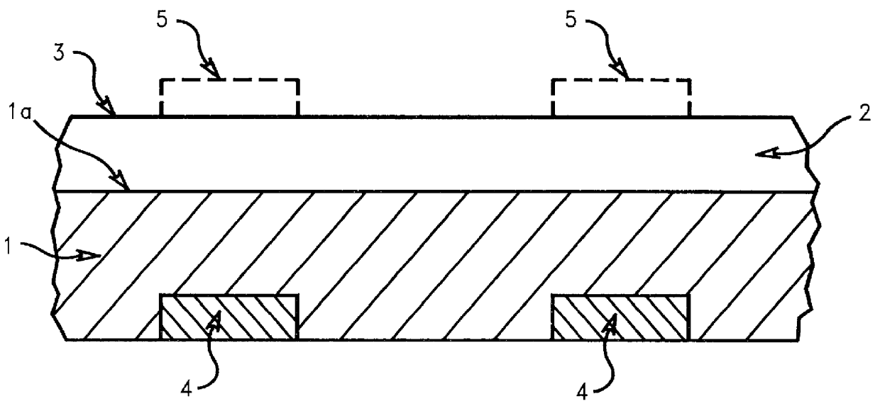
In alternative embodiments of the invention, a dielectric surface treatment can be used to either introduce a non-constituent element to the surface only of the high dielectric constant material which enhances the functioning of the high dielectric constant material or remove non-bulk contaminants from the surface of the high dielectric constant material.

While the invention has been described in terms of specific embodiments, it is evident in ...


PUM

PropertyMeasurementUnit
pressureaaaaaaaaaa
temperatureaaaaaaaaaa
dielectricaaaaaaaaaa

Abstract

This invention relates to a method for improving the chemical and electrical performance characteristics of a high dielectric constant material. The method comprises the steps of first obtaining a barium containing high dielectric constant material, the material having an upper surface and then modifying the surface chemistry of said upper surface by interacting said upper surface with a gas reactant in a closed environment. In a variant of the method, the gas reactant preferentially reacting with upper surface as compared to the bulk.

Description

The present invention relates to high dielectric capacitors which are useful in semiconductor devices. More particularly, the present invention relates to a method for producing high quality capacitors, as well as the structure of such capacitors.BACKGROUND OF INVENTIONMaterials having a permittivity of at least 20 are important for use in capacitors for advanced DRAMs such as the 1 Gbit generation and beyond. However, it has not been easy to maximize the overall storage charge of capacitors containing high dielectric constant materials. Events that occur during the fabrication process can reduce the final overall charge storage capability of the capacitor.Capacitor performance can be increased by reducing the capacitor leakage current. Leakage current is a stray current which flows across the surface of a high dielectric constant capacitor or alternatively through the capacitor.Leakage currents can cause unpredictable and detrimental changes in circuit conditions. It is therefore a...

Claims


Application Information

Patent Timeline
Patent Type & Authority Patents(United States)
IPC IPC(8): H01L21/02H01L21/316H01L21/311H01L21/306
CPCH01L21/31691H01L21/31122H01L21/02052H01L21/31111H01L28/55H01L21/02197H01L21/0206H01L21/02359H01L21/02337
Inventor DUNCOMBE, PETER R.KOTECKI, DAVID E.LAIBOWITZ, ROBERT B.NATZLE, WESLEYYU, CHIENFAN
Owner IBM CORP
Why Eureka
Try Eureka