Supercharge Your Innovation With Domain-Expert AI Agents!

Semiconductor device, method of fabricating the same, and electronic apparatus

Inactive Publication Date: 2000-05-02
SEIKO EPSON CORP
View PDF4 Cites 38 Cited by
  • Summary
  • Abstract
  • Description
  • Claims
  • Application Information

AI Technical Summary

Benefits of technology

In this method, the reinforcing member represents any part serving to prevent the film carrier tape from warping (for ensuring planarity). As such a reinforcing member, a so-called stiffener is used in most cases of semiconductor device fabrication.
In this method of the present invention, not only the semiconductor chip mounting step and the resin sealing step, but also the reinforcing member attaching step and the external electrode forming step can be carried out in a continuous reel-to-reel fashion, thereby increasing productivity and reducing manufacturing cost.
With this method, since the step of bonding the heat spreading member is also performed before the film carrier tape is punched out, continuous and efficient fabrication can be accomplished. The heat spreading member is used for efficiently dissipating heat from the semiconductor chip and bonded to the semiconductor chip depending on the amount of heat to be produced.

Problems solved by technology

However, since quality assurance and the handling of a bare chip are difficult, the chip is assembled in a package during semiconductor device fabrication.
Since the film carrier tape is liable to warp due to lack of rigidity, however, it is required to attach a reinforcing sheet (stiffener).
In this method, after the stiffener has been attached as mentioned above, the film packages must be handled individually in subsequent processes such as bump formation, resulting in trouble in fabrication.

Method used


Image

  • Semiconductor device, method of fabricating the same, and electronic apparatus
  • Semiconductor device, method of fabricating the same, and electronic apparatus
  • Semiconductor device, method of fabricating the same, and electronic apparatus

Examples


Embodiment Construction

Embodiments of the present invention will now be described below with reference to the accompanying drawings.

FIGS. 1A through 7 are diagrams illustrating the steps in the embodiment of the semiconductor device fabrication method of the present invention, and FIG. 8 shows the embodiment of a finished semiconductor device according to the present invention.

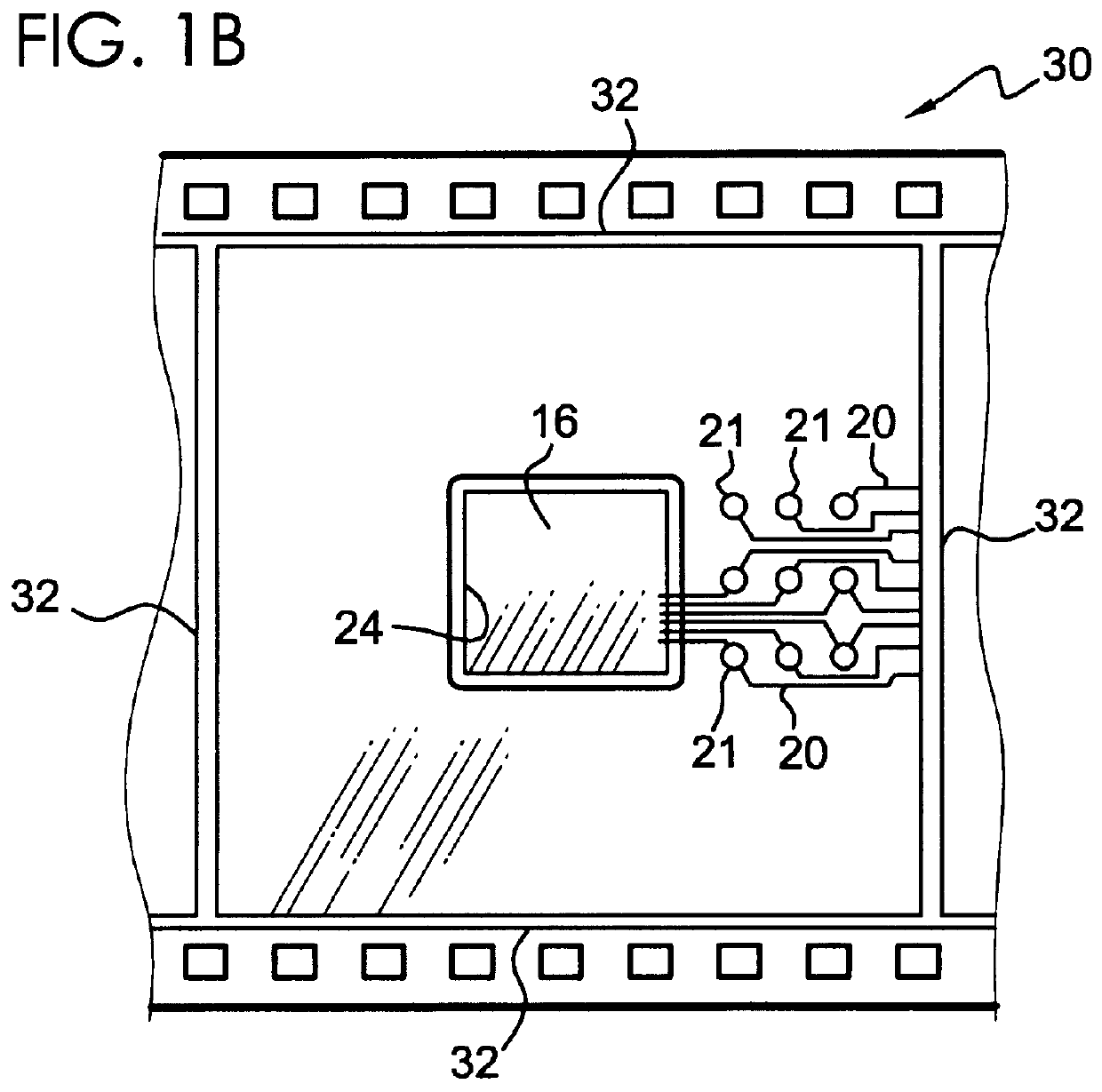
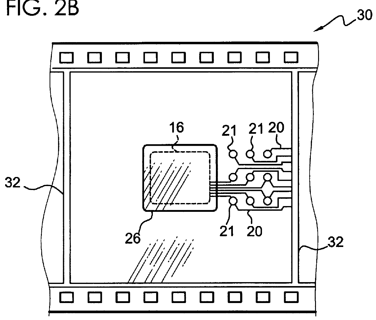
As shown in FIG. 8, a BGA package is applied to a semiconductor device 10. In this figure, the semiconductor device 10 comprises an insulating film 12, a plurality of leads 20 formed on the insulating film 12, a bump 14 formed on each of the leads 20, and a semiconductor chip 16. The bump 14 is used for an external electrode. Surface mounting can be implemented by using the plurality of bumps 14.

The insulating film 12 is formed by punching out a long film carrier tape 30 (see FIG. 1B), using the TAB technique in a process of fabrication. The insulating film 12 is formed to be larger than the semiconductor chip 16, and a device hole ...


PUM


Abstract

Method of fabricating semiconductor devices comprising the steps of: mounting a plurality of semiconductor chips on a film carrier tape; sealing each one of the semiconductor chips mounted on the film carrier type with epoxy resin; attaching an individual stiffener to the film carrier tape at a position corresponding to each one of the semiconductor chips; forming a plurality of bumps on the film carrier tape at a position corresponding to each one of the semiconductor chips; and punching out the film carrier tape into separate pieces of insulating film after above-described steps. In this method, each step is carried out on the film carrier tape running between supply and take-up reels.

Description

1. Field of the InventionThe present invention relates to a semiconductor device, a method of fabricating the same, and an electronic apparatus.2. Description of the Related ArtIn the microminiaturization of semiconductor devices, a bare chip mounting arrangement is regarded as an ideal form of assembly. However, since quality assurance and the handling of a bare chip are difficult, the chip is assembled in a package during semiconductor device fabrication. As one of the package forms meeting the need for high pin counts, a ball grid array (BGA) type package has been developed recently. On a substrate of the BGA type package, external terminal bumps are arranged in an area array to permit surface mounting.As one kind of BGA type package, there is a tape ball grid array (T-BGA) package in which a film carrier tape is used as a base in fabrication with a tape automated bonding (TAB) technique. In T-BGA packaging using the TAB technique, semiconductor chips can be assembled continuousl...

Claims


Application Information

Patent Timeline
IPC IPC(8): H01L21/02H01L23/34H01L23/495H01L21/60H01L23/36H01L23/48H01L23/498
CPCH01L23/36H01L23/49572H01L23/4985H01L24/86H01L2924/07802H01L2224/16H01L2224/7965H01L2924/01029H01L2924/01058H01L2924/01078H01L2924/01082H01L2924/15153H01L2924/1517H01L2924/15311H01L2924/1532H01L2924/19041H01L2924/19042H01L2924/19043H01L2924/01005H01L2924/01006H01L2924/01033H01L2924/01047H01L2924/014H01L2924/00H01L24/50H01L2924/12042H01L21/60
Inventor HASHIMOTO, NOBUAKI
Owner SEIKO EPSON CORP
Features
  • R&D
  • Intellectual Property
  • Life Sciences
  • Materials
  • Tech Scout
  • Unparalleled Data Quality
  • Higher Quality Content
  • 60% Fewer Hallucinations
Learn More