Process for control of the shape of the etch front in the etching of polysilicon

a technology of polysilicon and etching, which is applied in the direction of semiconductor devices, electrical apparatus, transistors, etc., can solve the problems of sculpturing of subsequently deposited layers of material, uneven thickness of teos sio.sub.2 collars, and increasing difficulty in controlling the shape of the surface being etched

Inactive Publication Date: 2000-06-13
APPLIED MATERIALS INC
View PDF20 Cites 148 Cited by
  • Summary
  • Abstract
  • Description
  • Claims
  • Application Information

AI Technical Summary

Problems solved by technology

Because trenches are present at the substrate surface, the thickness of the TEOS SiO.sub.2 collar is not uniform.
As device geometries continue to scale down, it becomes increasingly difficult to control the shape of the surface which is being etched.
If the shape of the etch front is not flat, sculpturing of subsequently deposited layers of material (e.g., during collar etch) may be difficult and the accuracy of interferometric endpoint determination during etch processing may be reduced.
Non-flat etch fronts make sculpturing of subsequently deposited layers of material (e.g., during collar etch) difficult and may reduce the accuracy of interferometric endpoint determination during etch processing.
Gases comprising oxygen are less preferred because oxygen dramatically reduces the etch selectivity toward polysilicon over the silicon nitride etch barrier.
The use of carbon-comprising gases may result in the formation of undesirable polymers.
Substrate bias reduces the selectivity of the plasma source gas to the silicon nitride etch barrier.

Method used


Image

  • Process for control of the shape of the etch front in the etching of polysilicon
  • Process for control of the shape of the etch front in the etching of polysilicon
  • Process for control of the shape of the etch front in the etching of polysilicon

Examples


example two

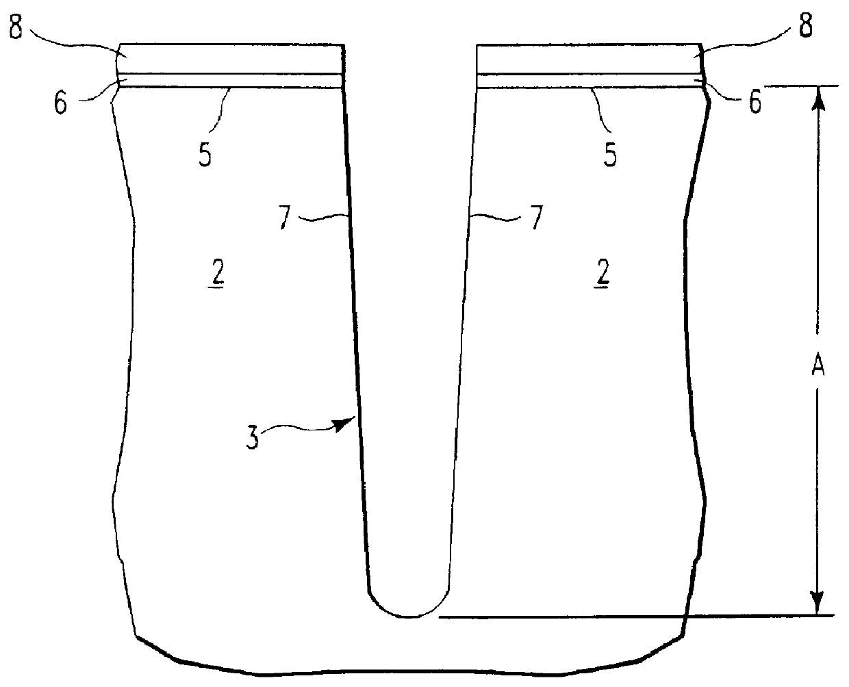
The structure described in Example One, above, and shown in FIG. 3 was provided (step a). A conformal dielectric film 10 was then formed overlying the silicon nitride etch barrier layer 8 and the sidewall 7 and bottom of the trench 3 (step b). The conformal dielectric film 10 was a multi-layered ONO film, as described in Example One. The trench 3 was then filled with a layer 12 of polysilicon overlying the conformal dielectric film 10 (step c). The above steps (a-c) were performed as described in Section IV and Example One, above, and illustrated in FIGS. 3-5.

Recess etchback of the polysilicon layer 12 (step d) was then performed to a predetermined depth within the trench, as illustrated in FIGS. 6a and 6b, using the plasma source gas composition and general process parameters described in Section III, above. This first etchback of polysilicon is referred to herein as "Recess Etch 1". Specific process parameters for Recess Etch 1 were as follows: Gas flow was 100 sccm SF.sub.6 and 1...


PUM


Abstract

The present disclosure pertains to our discovery that the use of a particular combination of etchant gases results in the formation of a substantially flat etch front for polysilicon etching applications. In general, the process of the invention is useful for controlling the shape of the etch front during the etchback of polysilicon. Typically, the process comprises isotropically etching the polysilicon using a plasma produced from a plasma source gas comprising a particular combination of reactive species which selectively etch polysilicon. The plasma source gas comprises from about 80% to about 95% by volume of a fluorine-comprising gas, and from about 5% to about 20% by volume of an additive gas selected from a group consisting of a bromine-comprising gas, a chlorine-comprising gas, an iodine-comprising gas, or a combination thereof. One preferred mixture is SF6, Cl2 and HBr. A preferred method of the invention, used to perform recess etchback of a polysilicon-filled trench in a substrate, comprises the following steps: a) providing a trench 3 formed in a semiconductor structure, wherein the structure includes a substrate 2, at least one gate dielectric layer 6 overlying a surface of the substrate, and at least one etch barrier layer 8 overlying the gate dielectric layer; b) forming a conformal dielectric film 10 overlying the etch barrier layer and the sidewall and bottom of the trench; c) filling the trench with a layer of polysilicon 12 which overlies the conformal dielectric film; and d) isotropically etching the polysilicon back to a predetermined depth within the trench using a plasma produced from the invention plasma source gas. Also disclosed herein is a method of forming a trench capacitor in a single-crystal silicon substrate, the trench capacitor including a dielectric collar and a buried strap.

Description

1. Field of the InventionThe present invention pertains to a process for control of the shape of the etch front in polysilicon etching applications. The present invention also pertains to a method for recess etchback of a polysilicon-filled trench formed in a substrate, as well as a method for forming a polysilicon-filled trench capacitor in a single-crystal silicon substrate, the trench capacitor including a dielectric collar and a buried strap.2. Brief Description of the Background ArtThere are a number of methods described in the art for etching polysilicon films and for the etchback of polysilicon. Several of these methods are described below.U.S. Pat. Nos. 4,895,810 and 5,182,234, issued Jan. 23, 1990 and Jan. 26, 1993, respectively, to Meyer and Hollinger et al., disclose depositing a dopant-opaque layer of polysilicon on a gate oxide on the upper substrate surface to serve as a pattern definer during fabrication of a device, to provide control over successive P and N doping s...

Claims


Application Information

Patent Timeline
Patent Type & Authority Patents(United States)
IPC IPC(8): H01L21/02H01L21/763H01L21/334H01L21/70H01L21/3213H01L21/8242H01L21/302H01L21/3065H01L27/108
CPCH01L21/32137H01L29/66181H01L27/10861H01L21/763H10B12/038
Inventor LILL, THORSTENGRIMBERGEN, MICHAEL
Owner APPLIED MATERIALS INC
Why Eureka
Try Eureka