Sense amplifier for high-density imaging array

a high-density imaging array and amplifier technology, applied in the field of integrated circuit technology of high-density imaging arrays, can solve the problems of inability to fit in the width available or the design of traditional amplifiers is too large or noisy

Inactive Publication Date: 2000-08-01
FOVEON
View PDF32 Cites 129 Cited by
  • Summary
  • Abstract
  • Description
  • Claims
  • Application Information

AI Technical Summary

Problems solved by technology

Traditional amplifier designs either have too much noise or cannot be made to fit in the width available.

Method used


Image

  • Sense amplifier for high-density imaging array
  • Sense amplifier for high-density imaging array
  • Sense amplifier for high-density imaging array

Examples


Embodiment Construction

Those of ordinary skill in the art will realize that the following description of the present invention is illustrative only and not in any way limiting. Other embodiments of the invention will readily suggest themselves to such skilled persons.

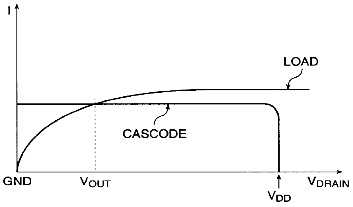
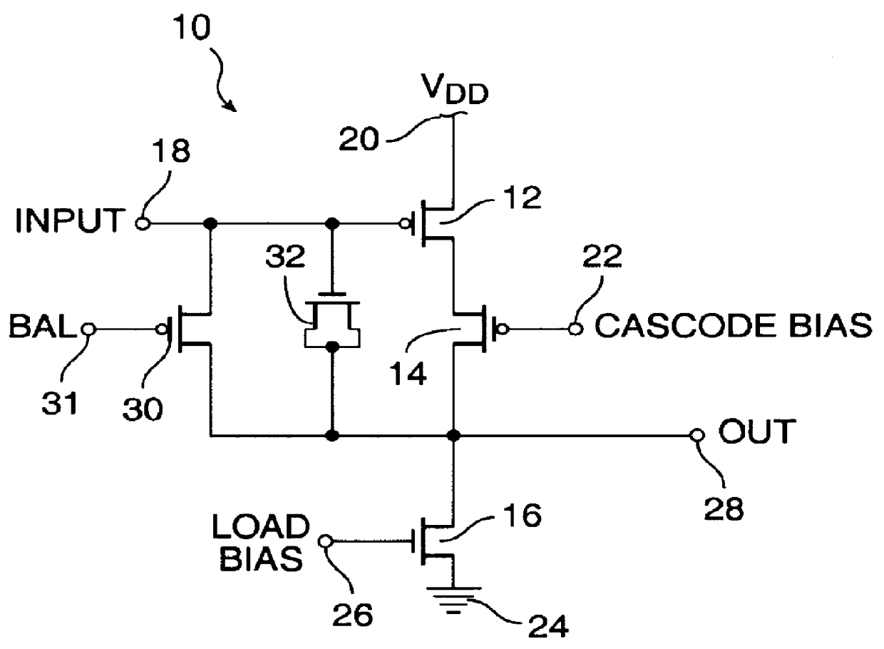
The present invention teaches an amplifier design that achieves low noise, high gain, low power dissipation, and a compressive input-output characteristic, all in a narrow width. The schematic diagram of such a sense amplifier 10 is shown in FIG. 1. Sense amplifier 10 comprises input transistor 12, cascode transistor 14, and load transistor 16. In the embodiment of FIG. 1, input transistor 12 is a P-Channel MOS transistor, cascode transistor 14 is a P-Channel MOS transistor, and load transistor 16 is an N-Channel MOS transistor.

Input transistor 12 has its gate connected to input line 18, its source connected to Vdd rail 20, and its drain connected to the source of cascode transistor 14. The gate of cascode transistor 14 is connected to a casc...


PUM


Abstract

A sense amplifier comprises an input node and an output node. An input transistor has a gate connected to the input node, a source connected to a first supply voltage rail, and a drain. A cascode transistor has a gate connected to a cascode node, a source connected to the drain of the input transistor, and a drain connected to the output node. A load transistor has a gate connected to a bias node, a drain connected to the output node, and a source connected to a second supply voltage rail. The gates of the cascode transistor and the load transistor are biased such that the input transistor and the cascode transistor are operated near their threshold and the load transistor is operated above threshold. In a presently preferred embodiment of the present invention, the input transistor and the cascode transistor of the sense amplifier are wide and short, such that they operate in below threshold, whereas the load transistor is made long and relatively narrow, so that it operates above threshold.

Description

1. Field of the InventionThe present invention relates to integrated circuit technology and imaging array technology and amplifier technology for use in integrated circuit applications. More particularly, the present invention relates to a high density imaging array integrated circuit including a sense amplifier for use in such an array.2. The Prior ArtSense amplifier circuits in general are known in the prior art. Sense amplifier circuits for use in imaging arrays are also known in the prior art.A high-density photosensing imager may be realized by an array of bipolar transistors with bases capacitively coupled to sense lines, as previously disclosed by Mead et al. in U.S. Pat. Nos. 5,097,305, 5,260,592, and 5,324,958. In such an imager it is necessary to construct a sense amplifier that has a gain of 1000 or greater. It would be advantageous for such a sense amplifier to fit into a width of one pixel in the imager array (6 microns in a 1 micron process) so as to be able to provide...

Claims


Application Information

Patent Timeline
Patent Type & Authority Patents(United States)
IPC IPC(8): G11C7/06G11C27/02G11C27/00
CPCG11C7/067G11C27/024
Inventor MEAD, CARVER A.DELBRUCK, TOBIAS
Owner FOVEON
Why Eureka
Try Eureka