
Semiconductor device and method of manufacturing the same, circuit board, and electronic instrument

a semiconductor and semiconductor technology, applied in the direction of manufacturing tools, printed circuit non-printed electric components association, electrical apparatus casings/cabinets/drawers, etc., can solve the problems of external electrode stress and cracks forming in external electrodes

Inactive Publication Date: 2000-08-01
ADVANCED INTERCONNECT SYST LTD
View PDF14 Cites 46 Cited by
  • Summary
  • Abstract
  • Description
  • Claims
  • Application Information

AI Technical Summary

Benefits of technology

According to the present invention, since protrusions are formed in the internal wall surfaces of the penetrating holes, deformation is easier than with flat internal wall surfaces. Therefore, stress caused by differences in the coefficient of thermal expansion with the circuit board (thermal stress) and mechanical stress applied to the circuit board from the outside can be absorbed. In this way, the occurrence of cracks in the external electrodes can be prevented.
With a semiconductor device fabricated according to the present invention, the diameter d of the base portion of the external electrodes is related to the diameter .phi. of the projecting portion by .phi..ltoreq.d. In other words, the diameter of the external electrodes is not squeezed by the penetrating holes, and no necking occurs. Therefore, stress caused by differences in the coefficient of thermal expansion with the circuit board (thermal stress) and mechanical stress applied from outside the circuit board is not concentrated, and as a result the occurrence of cracks in the external electrodes can be prevented.

Problems solved by technology

With a semiconductor device to which a package of this construction is applied, after mounting on the circuit board, because of the difference in coefficient of thermal expansion between the circuit board and semiconductor device, a stress may be applied to the external electrodes, and cracks may form in the external electrodes.

Method used


Image

  • Semiconductor device and method of manufacturing the same, circuit board, and electronic instrument
  • Semiconductor device and method of manufacturing the same, circuit board, and electronic instrument
  • Semiconductor device and method of manufacturing the same, circuit board, and electronic instrument

Examples


first embodiment

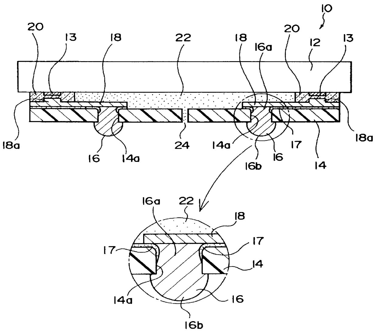
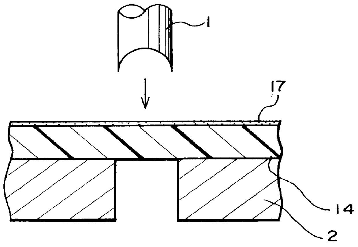
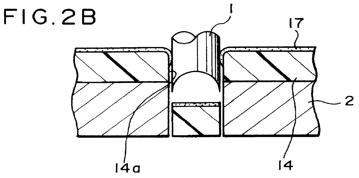
FIG. 1 shows a first embodiment of the semiconductor device. A semiconductor device 10 comprises a semiconductor chip 12, being an example of a semiconductor chip, and an insulating film 14, being an example of a substrate, to which the CSP type of package is applied. On the insulating film 14 are formed external electrodes 16, and the semiconductor chip 12 has a plurality of electrodes 13. In FIG. 1, the electrodes 13 are formed on only two opposite sides of the semiconductor chip 12, but as is well known, may equally be formed on four sides.

The insulating film 14 is formed of a polyimide resin or the like, and has a plurality of penetrating holes 14a. As the substrate formed of polyimide resin may be used one such that for example:

Coefficient of thermal expansion=12 ppm / .degree. C.

Modulus of elasticity=900 kg / mm.sup.2

Or one such that:

Coefficient of thermal expansion=20 ppm / .degree. C.

Modulus of elasticity=302 kg / mm.sup.2

To one surface of the insulating film 14 is adhered a wiring ...

second embodiment

FIG. 4 shows a second embodiment of the semiconductor device. This semiconductor device 110 includes a semiconductor chip 112, an insulating film 14 being an example of a substrate (the same construction as the first embodiment), and aplurality of external electrodes 16 (the same construction as the first embodiment). Bumps 113 are provided on a plurality of electrodes (not shown in the drawing) of the semiconductor chip 112. The bumps 113 are commonly gold ball bumps or gold plating bumps, but may equally be solder balls. The insulating film 14 is formed to be larger than the semiconductor chip 112.

On one surface of the insulating film 14 is adhered a conductive member 118. The conductive member 118 is formed as the wiring pattern 18 shown in FIG. 1 with the projections 18a omitted, and is attached to the insulating film 14 with an adhesive 17.

The electrical connection of the bumps 113 and conductive member 118 is achieved by an anisotropic conductive material 120 provided over the...

third embodiment

FIG. 5 shows a third embodiment of the semiconductor device of the present invention. The semiconductor device 30 shown in this figure has a wiring pattern 38 and electrodes 33 of a semiconductor chip 32 connected by wires 40. The wiring pattern 38 is formed by adhesion to a substrate 34 with an adhesive 37 interposed. The substrate 34 may be an insulating film in the same way as in the first embodiment, or a printed circuit board.

On the surface of the substrate 34 on which the wiring pattern 38 is formed, a stress relieving layer 42 is provided. The stress relieving layer 42 is formed of a material such as may be selected as the resin 22 in the first embodiment. The stress relieving layer 42 is affixed by means of an adhesive 46 to the surface opposite to the surface having the electrodes 33 of the semiconductor chip 32.

In the substrate 34 are formed penetrating holes 34a. Through these penetrating holes 34a, external electrodes 36 are formed on the wiring pattern 38. In more detai...


PUM

PropertyMeasurementUnit
Diameteraaaaaaaaaa
Electrical conductoraaaaaaaaaa
Elasticityaaaaaaaaaa

Abstract

The semiconductor device comprises an insulating film in which penetrating holes are formed, a semiconductor chip having electrodes, a wiring pattern adhered by an adhesive over a region including penetrating holes on one side of the insulating film and electrically connected to the electrodes of the semiconductor chip, and external electrodes provided on the wiring pattern through the penetrating holes and projecting from the surface opposite to the surface of the substrate on which the wiring pattern is formed. Part of the adhesive is drawn in to be interposed between the penetrating holes and external electrodes.

Description

1. Field of the InventionThe present invention relates to a semiconductor device and method of manufacture thereof, a circuit board, and an electronic instrument.2. Description of Related ArtWith the recent increasingly compact nature of electronic instruments, there is a demand for semiconductor device packages appropriate for high-density mounting. In response to this, surface-mounted packages have been developed, such as Ball Grid Array (BGA) and Chip Scale / Size Package (CSP). With such surface-mounted packages, a substrate is often used on which a wiring pattern for connection to the semiconductor chip is formed. Penetrating holes are formed in substrate, and external electrodes are often formed so as to project through these penetrating holes from the surface opposite to that of the wiring pattern.With a semiconductor device to which a package of this construction is applied, after mounting on the circuit board, because of the difference in coefficient of thermal expansion betw...

Claims


Application Information

Patent Timeline
IPC IPC(8): H01L21/56H01L21/48H01L21/02H01L23/498H01L23/48H01L23/12
CPCH01L21/486H01L24/13H01L23/13H01L23/16H01L23/24H01L23/3114H01L23/49816H01L23/49827H01L23/562H01L24/10H01L24/81H01L24/83H05K1/112H01L24/32H01L24/29H01L21/563H01L2224/13099H01L2224/16237H01L2224/32225H01L2224/48091H01L2224/48227H01L2224/73203H01L2224/73265H01L2224/81801H01L2224/83102H01L2224/83192H01L2224/83194H01L2224/8385H01L2224/92125H01L2924/01004H01L2924/01029H01L2924/01033H01L2924/0105H01L2924/01078H01L2924/01079H01L2924/01082H01L2924/07802H01L2924/15151H01L2924/15184H01L2924/15311H01L2924/19041H01L2924/19043H05K3/3457H05K3/386H05K3/4038H05K2201/0305H05K2201/0394H01L24/48H01L2224/2919H01L2924/01005H01L2924/01006H01L2924/014H01L2924/0665H01L2224/16225H01L2224/73204H01L2224/48465H01L2924/12041H01L2924/07811H01L2924/00014H01L2924/00012H01L2924/00H01L2924/3512H01L24/16H01L24/73H01L2224/0401H01L2224/13H01L2224/1329H01L2224/133H01L2924/12042H01L2924/15183H01L2924/181H01L2924/351H01L2224/45099H01L2224/05599H01L2224/85399H01L2224/45015H01L2924/207H01L2224/05099H01L23/12H01L2224/05001H01L2224/05022H01L2224/05548H01L2224/05647
Inventor HASHIMOTO, NOBUAKI
Owner ADVANCED INTERCONNECT SYST LTD
Features
  • Generate Ideas
  • Intellectual Property
  • Life Sciences
  • Materials
  • Tech Scout
  • Unparalleled Data Quality
  • Higher Quality Content
  • 60% Fewer Hallucinations
Learn More