Optimum buffer placement for noise avoidance

Inactive Publication Date: 2000-09-12
GLOBALFOUNDRIES INC
View PDF5 Cites 176 Cited by
  • Summary
  • Abstract
  • Description
  • Claims
  • Application Information

AI Technical Summary

Problems solved by technology

Often, when a signal propagates within an integrated circuit noise is induced into the signal.
Therefore, dynamic logic families are more susceptible to noise failure than conventional static logic.
Even though these techniques are adequate for analysis they cannot be utilized to optimize a design.
As a result of the increase in the coupling capacitance, a transient voltage or current on a conductor can adversely affect neighboring signals.
This phenomenon can have a detrimental effect on circuit response.
For example, a coupled noise pulse can erroneously switch the state of a transistor which is required to be in a different state.
Undesired switching of a single transistor can "lock up" an entire computer system rendering the computer system unresponsive to all input.
Low switching threshold voltages make prevention of faulty switching of a transistor due to coupling noise a significant concern.
Presently, greater utilization of noise analysis in the design phase of integrated circuits having dynamic lo

Method used


Image

  • Optimum buffer placement for noise avoidance
  • Optimum buffer placement for noise avoidance
  • Optimum buffer placement for noise avoidance

Examples


Embodiment Construction

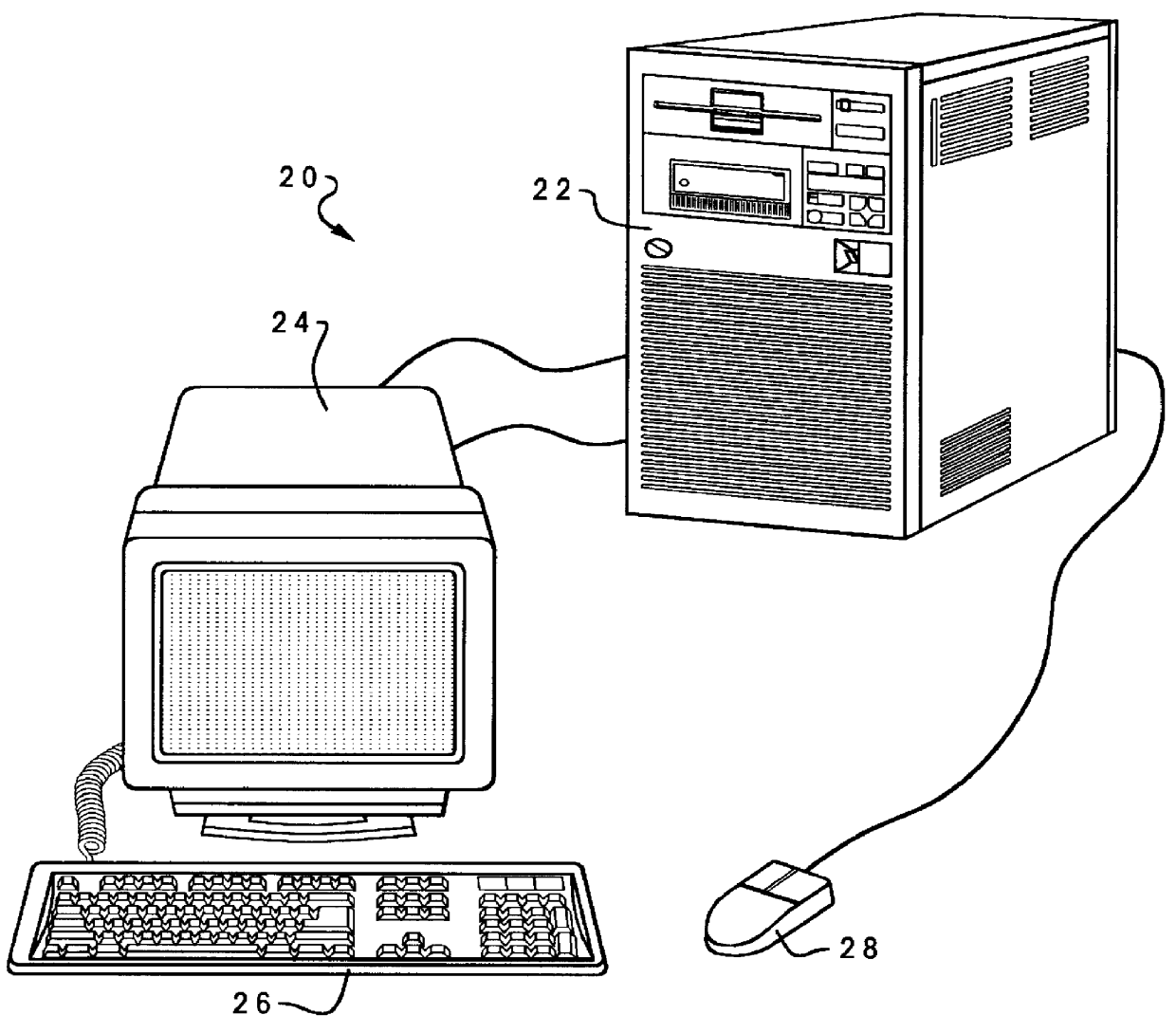
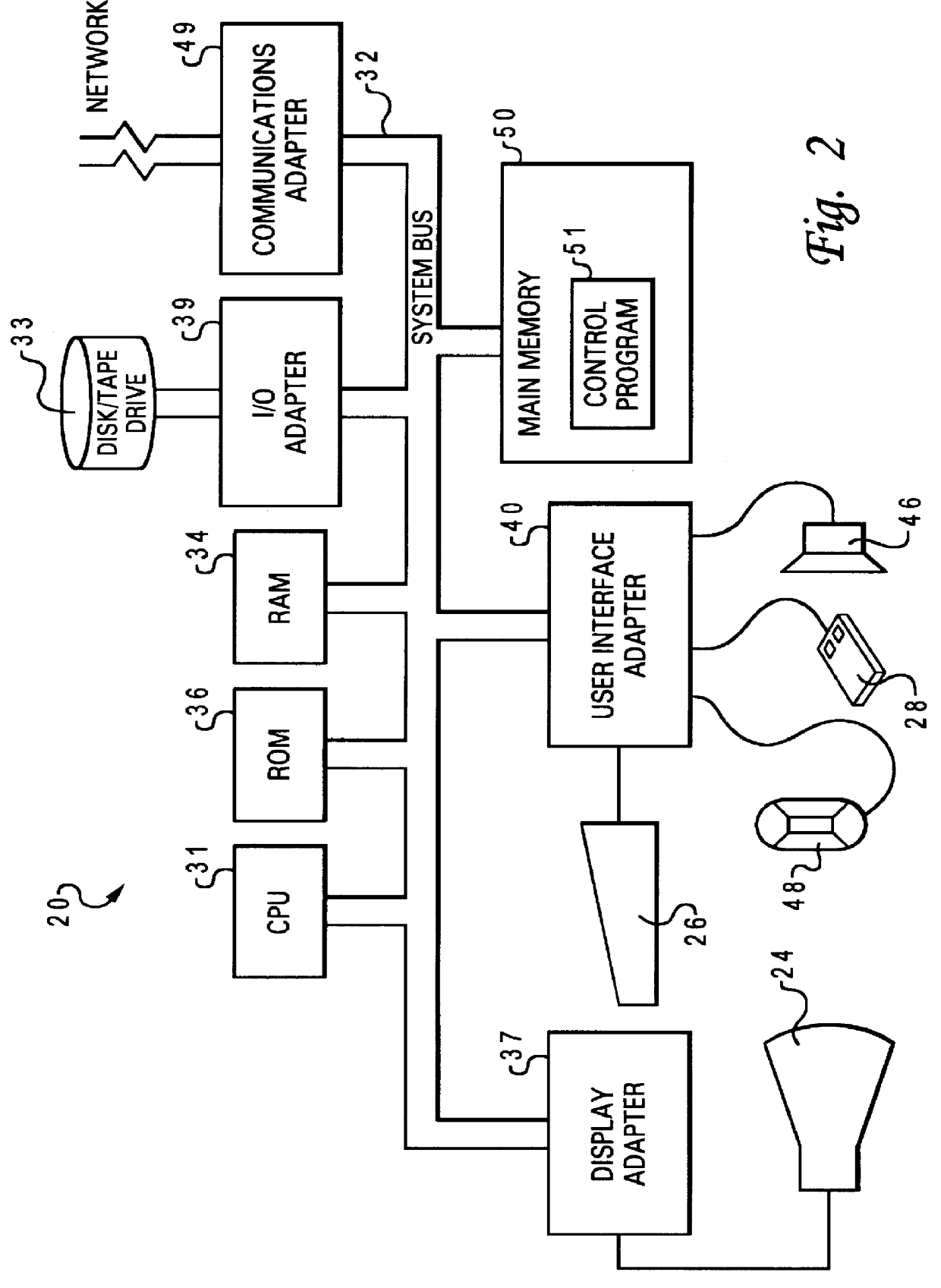
With reference now to the figures and in particular with reference to FIG. 1, there is depicted a pictorial representation of a computer system which may be utilized to implement a preferred embodiment of the present invention. A computer system 20 is depicted that includes a system unit 22, a video display terminal 24, a keyboard 26, and a mouse 28. Keyboard 26 is that part of computer system 20 that resembles a typewriter keyboard and enables a user to control particular aspects of the computer. Because information flows in one direction from keyboard 26 to system unit 22, keyboard 26 functions as an input-only device.

Functionally, keyboard 26 represents half of a complete input / output device, the output half being video display terminal 24. Keyboard 26 includes a standard set of printable characters presented in a QWERTY pattern typical of most typewriters. In addition, keyboard 26 includes a calculator-like numeric keypad at one side. Some of these keys, such as the "control," "...


PUM


Abstract

A method for optimal insertion of buffers into an integrated circuit design. A model representative of a plurality of circuits is created where each circuit has a receiving node coupled to a conductor and a source. A receiving node is selected from the modeled plurality of circuits and circuit noise is calculated for the selected receiving node utilizing the circuit model. If the calculated circuit noise exceeds an acceptable value an optimum distance is computed from the receiving node on the conductor for buffer insertion. In a multi-sink circuit merging of the noise calculation for the two receiving circuits must be accomplished. If an intersection of conductors exists between the receiving node and the optimum distance a set of candidate buffer locations is generated. The method then prunes inferior solutions to provide an optimal insertion of buffers.

Description

1. Technical FieldThe present invention relates in general to an improved integrated circuit design method and in particular to an improved integrated circuit design method for optimum insertion of buffers in an integrated circuit containing single-sink and multi-sink circuits. Still more particularly, the present invention relates to a design method which determines an optimum distance from a sink in multi-sink circuits for a buffer location and generates candidate solutions and selects optimum buffer locations from the candidate locations.2. Description of the Related ArtOften, when a signal propagates within an integrated circuit noise is induced into the signal. The signal can be restored to its original shape by "repowering" the signal utilizing simple amplifiers called "buffers".In designing an integrated circuit, the physical layout is accomplished in view of all the pertinent design constraints. Generally, after the layout or geographical planning of a semiconductor chip is ...

Claims


Application Information

Patent Timeline
IPC IPC(8): G06F17/50
CPCG06F17/505G06F17/5068G06F30/327G06F30/39G06F30/398
Inventor ALPERT, CHARLES JAYQUAY, STEPHEN THOMASDEVGAN, ANIRUDH
Owner GLOBALFOUNDRIES INC
Why Eureka
Try Eureka