Fabrication of interconnects with two different thicknesses

a technology of interconnections and thicknesses, applied in the direction of basic electric elements, semiconductor devices, electrical apparatus, etc., can solve the problems of complex use of separate processes for their fabrication, noise through capacitive coupling between, and add complexity to lithographic and other manufacturing processes

Inactive Publication Date: 2000-10-24
IBM CORP
View PDF12 Cites 20 Cited by
  • Summary
  • Abstract
  • Description
  • Claims
  • Application Information

AI Technical Summary

Benefits of technology

It is another object of the invention to provide a damascene process which can provide conductors of differing thicknesses without being compromised or complicated by stringent requirements for registration of plural masks.
It is a further object of the invention to provide a structure for an integrated circuit device in which conductor dimensions may be optimized in the array and support regions thereof for noise immunity and increased signal propagation speed.

Problems solved by technology

Unfortunately, the circuit requirements are generally different for the array and support regions of the chip and hence ideally would require different processes during manufacture.
For example, the word lines or bit lines in a functional region of the integrated circuit such as an array portion of a memory need not carry large currents but run generally parallel to each other at close spacing and cannot generally be reduced in length for a given chip or partitioning; leading to noise through capacitive coupling between them.
However, these conductors are often in the same metal level and the use of separate processes for their fabrication is complicated by at least required masking beyond the procedures involved in the plural separate processes themselves.
Previously proposed methods add complexity to lithographic and other manufacturing processes and can adversely affect manufacturing yield.
Registration of these steps is very difficult and expensive and very slight misregistration can greatly compromise manufacturing yield and / or circuit performance.
If conductors of different cross-sectional areas are fabricated with a single thickness (e.g. either a single mask damascene process of patterned surface deposition), the width necessary to significantly reduce resistance would increase capacitance due to the increased area, limiting the gains in signal propagation speed from decreased resistance and, perhaps more importantly, would require increased chip area such that currently available lithographic processes cannot be fully exploited to increase array density and device counts.
Surface deposition and patterning yields conductors which are much less robust and uniform and which may become even more delicate and subject to shorting and metal migration (which tends to open connections in a largely unpredictable manner) if height of the conductors is increased.
The surface connections so formed are particularly vulnerable to damage during mask or resist removal or other required processing.
Further, surface conductors of differing height present severe surface topology which may complicate or compromise subsequent lithographic processes (e.g. exposure focus).

Method used


Image

  • Fabrication of interconnects with two different thicknesses
  • Fabrication of interconnects with two different thicknesses
  • Fabrication of interconnects with two different thicknesses

Examples


Embodiment Construction

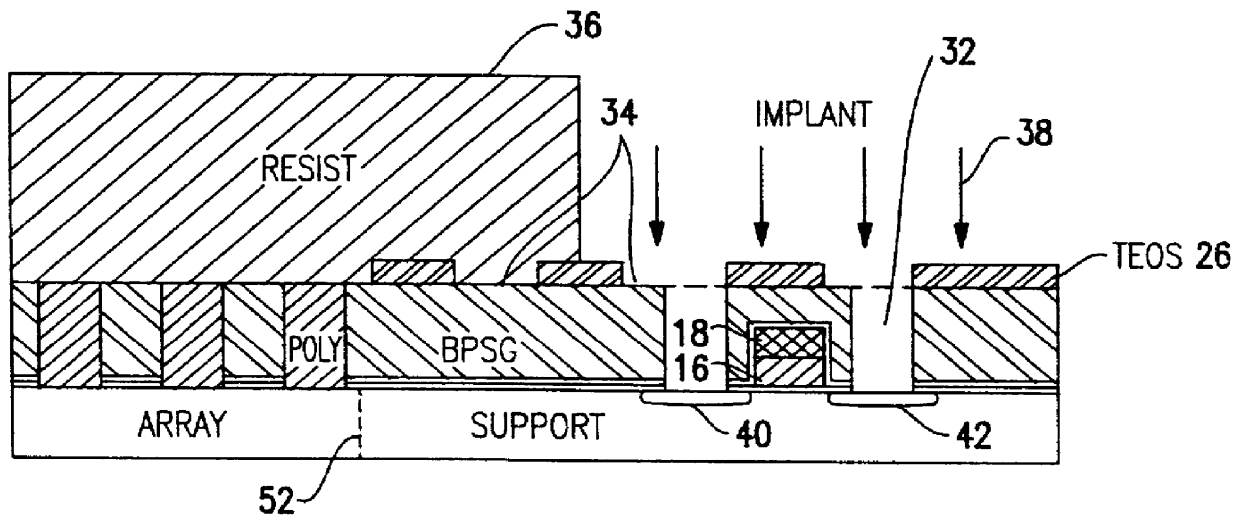
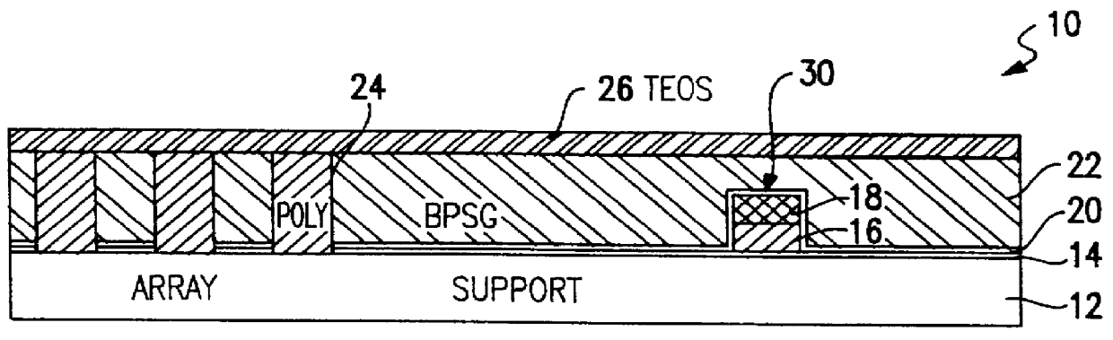
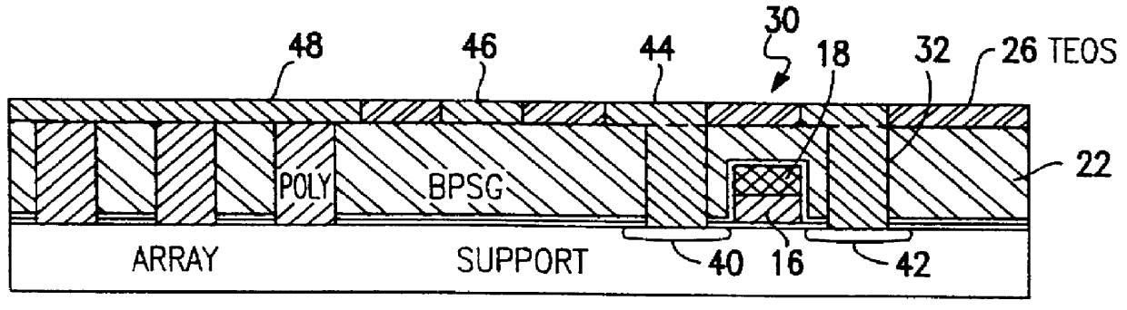
Referring now to the drawings, and more particularly to FIGS. 1, 4 and 7, there is shown, in cross-section, a partially completed portion 10 of a structure of an exemplary dynamic random access memory (DRAM) in a region including a boundary (generally depicted at 52) between an array portion or region including a large plurality of storage cells and a support portion or region including addressing circuits, decoders, sense amplifiers and the like in which only a single exemplary field effect transistor 30 is shown for clarity. It should be understood that these illustrations and the portions of structure repeated in the remainder of the Figures is generalized in the interest of clarity and details not important to the practice of the invention are thus omitted. Accordingly, while FIGS. 1-3 are illustrative of structure over which the present invention provides an improvement, no portion of any Figure is admitted to be prior art as to the present invention.

The structures of FIGS. 1, ...


PUM


Abstract

Provision of differential etching of layers by, for example, an etch stop layer or implantation, allows a second trough etch to be performed in accordance with a block-out mask (which does not require high accuracy of registration) to provide troughs or recesses of different depths in layers of insulator. When the recesses or troughs are filled by metal deposition and patterned by planarization in accordance with damascene processing, structurally robust conductors of differing thicknesses may be achieved and optimized to enhance noise immunity and / or signal propagation speed in different functional regions of an integrated circuit such as the so-called array and support portions of a dynamic random access memory.

Description

1. Field of the InventionThe present invention generally relates to integrated circuit devices formed at high integration density and, more particularly, to formation of circuits which may have widely varying current-carrying, signal propagation time and noise immunity requirements for respective circuits and / or sub-systems which may be included therein such as in dynamic random access memories (DRAMs).2. Description of the Prior ArtManufacture and design of integrated circuits has greatly increased in sophistication in recent years, particularly in regard to increase of integration density. Increased integration density leads to economic advantages as increased numbers of devices and circuits may be placed on a single chip and / or within a single package (which may include a plurality of chips). Performance improvements such as reduced signal propagation time and noise immunity can usually be achieved as integration density is increased due to reduction in length of signal paths, ca...

Claims


Application Information

Patent Timeline
Patent Type & Authority Patents(United States)
IPC IPC(8): H01L21/768H01L21/70H01L21/02H01L21/60H01L21/8242
CPCH01L21/76807H01L21/76814H01L21/76897H01L21/76825H01L27/10894H01L27/10882H10B12/48H10B12/09
Inventor GAMBINO, JEFFREY P.JASO, MARKWONG, HING
Owner IBM CORP
Why Eureka
Try Eureka