Method to selectively fill recesses with conductive metal

Inactive Publication Date: 2000-10-31
GLOBALFOUNDRIES INC
View PDF19 Cites 396 Cited by
  • Summary
  • Abstract
  • Description
  • Claims
  • Application Information

AI Technical Summary

Benefits of technology

An object of the present invention is to provide a process that permits reducing the time required for CMP of plated damascene structures, thereby increasing the thruput. An object of this invention is

Problems solved by technology

Also, insulator gap fill and planarization may be more problematic.
During metal CMP, the additional time needed to remove the excess metal overburden on the overplated smaller features causes dishing on the larger features.
Also, because of the prolonged polishing times, insulator adjacent may become severely eroded.
Severe dishing and insulator erosion i

Method used


Image

  • Method to selectively fill recesses with conductive metal
  • Method to selectively fill recesses with conductive metal
  • Method to selectively fill recesses with conductive metal

Examples


Embodiment Construction

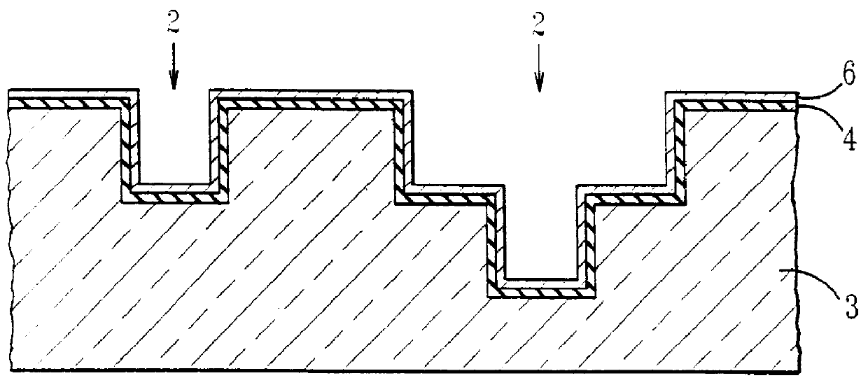
In accordance with the present invention, recesses 2 such as troughs and vias are provided on at least one major surface of a semiconductor substrate (not shown). Typical semiconductor substrates include silicon and group III-V semiconductors. Electrical insulation 3 is provided over the major surface and in the recesses such as silicon dioxide which can be thermally grown or deposited such as by chemical vapor deposition or physical vapor deposition. Typically, the insulating layer is about 2000 to about 30,000 .ANG. thick, and more typically about 4000 to about 20,000 .ANG. thick.

Next, a conductive barrier 4 is provided over the insulating layer. Preferably, a layer of tantalum nitride is first sputter deposited over the insulating layer to a thickness of about 15 to about 500 .ANG. and more typically to a thickness of about 50 to about 300 .ANG. to act as adhesion promoting layer between the insulating layer and subsequently to be applied tantalum layer. Next a tantalum layer is ...


PUM

PropertyMeasurementUnit
Thicknessaaaaaaaaaa
Currentaaaaaaaaaa
Electrical conductoraaaaaaaaaa

Abstract

Recesses in a semiconductor structure are selectively plated by providing electrical insulating layer over the semiconductor substrate and in the recesses followed by forming a conductive barrier over the insulating layer; providing a plating seed layer over the barrier layer; depositing and patterning a photoresist layer over the plating seed layer; planarizing the insulated horizontal portions by removing the horizontal portions of the seed layer between the recesses; removing the photoresist remaining in the recesses; and then electroplating the patterned seed layer with a conductive metal using the barrier layer to carry the current during the electroplating to thereby only plate on the seed layer. In an alternative process, a barrier film is deposited over recesses in an insulator. Then, relatively thick resists are lithographically defined on the field regions, on top of the barrier film over the recesses. A plating base or seedlayer is deposited, so as to be continuous on the horizontal regions of the recesses in the insulator, but discontinuous on their surround wall. The recesses are then plated using the barrier film without seedlayers at the periphery of the substrate wafers for electrical contact. After electroplating, the resist is removed by lift-off process and exposed barrier film is etched by RIE method or by CMP. Also provided is a semiconductor structure obtained by the above processes.

Description

The present invention is concerned with a process for fabricating metal wires in an integrated circuit. More particularly, the present invention is concerned with using a highly conducting barrier film to conduct electrical current and selectively plate recesses such as troughs and vias in a substrate. In particular, the present invention provides methods for the fabrication of multilevel wiring for chip interconnections. This is achieved by selectively plating recesses in a semiconductor substrate with conductive metal such as copper or gold. Only the trenches and vias in the insulator are plated. No plating occurs in the field regions above the recesses in the substrate. This selective deposition process reduces the subsequent polishing time for removing undesired plated metal overburden. Moreover, the present invention minimizes the problem of "dishing" as well as minimizing the erosion of the dielectric layer adjacent to the isolated conductive features or regions. Moreover, the...

Claims


Application Information

Patent Timeline
IPC IPC(8): H01L21/768H01L21/70C25D5/02C23C18/31C25D7/12H01L21/288H01L21/3205
CPCH01L21/76807H01L21/76843H01L21/76865H01L21/76873H01L21/76879H01L21/2885H01L2924/0002H01L2924/00H01L21/3205
Inventor UZOH, CYPRIAN EMEKAGRECO, STEPHEN EDWARD
Owner GLOBALFOUNDRIES INC
Why Eureka
Try Eureka