Semiconductor device

a technology of semiconductors and semiconductors, applied in static indicating devices, instruments, optics, etc., can solve the problems of difficult to realize a tft having such high speed performance, difficult to constitute an electric circuit requiring high frequency driving, such as a logic circuit, by tfts using presently employed silicon thin films,

Inactive Publication Date: 2000-11-14
SEMICON ENERGY LAB CO LTD
View PDF5 Cites 218 Cited by
  • Summary
  • Abstract
  • Description
  • Claims
  • Application Information

AI Technical Summary

Problems solved by technology

However, a technique for forming TFTs capable of realizing the plan has not been established.
The reason is that it is difficult to constitute an electric circuit requiring high frequency driving, such as a logic circuit, by TFTs using presently employed silicon thin films.
However, it is difficult to realize a TFT having such high speed performance that the TFT can constitute a logic circuit, by these silicon thin films.
Although the operating speed of a TFT can be tentatively improved by decreasing the size of the TFT, the reduction of a channel length (or gate length) causes a short channel effect, so that a trouble such as lowering of a drain withstand voltage occurs.
Thus, in the case of a TFT using a conventional silicon thin film, the improvement of an operating speed by a scaling law reaches the limit, and it is difficult to further raise the operating speed in view of reliability.
Also, ther

Method used


Image

  • Semiconductor device
  • Semiconductor device
  • Semiconductor device

Examples


embodiment 2

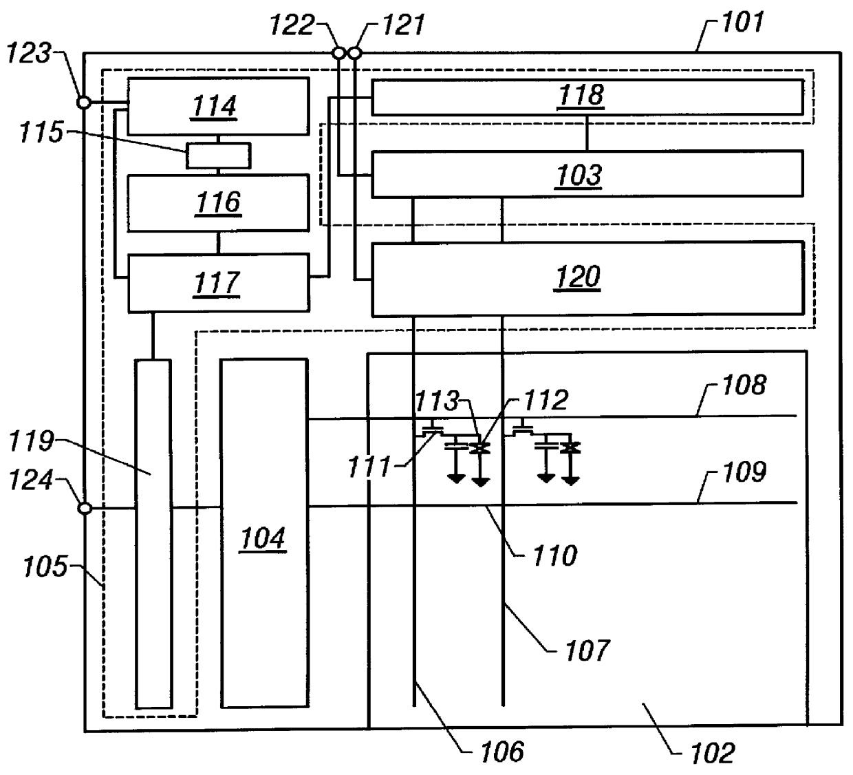
In reference to this embodiment, FIG. 6A is a sectional view showing a CMOS structure as a basic structure for constituting the source line driver circuit 103, the gate line driver circuit 104, and the logic circuit 105 in the active matrix display shown in FIG. 1. FIG. 6B is a sectional view showing the pixel TFT 111 and the pixel region 110 constituting the pixel matrix circuit 102. Incidentally, the structure shown in this embodiment is merely one example, and does not limit the present invention.

First, a CMOS structure in which an N-channel TFT 601 and a P-channel TFT 602 are complementarily combined with each other, will be described. The N-channel TFT 601 and the P-channel TFT 602 have substantially the same structure.

In FIG. 6A, 603 denotes a quartz substrate, 604 and 606 denote respectively a source region and a drain region of the N-channel TFT, and 605 and 607 denote respectively a source region and a drain region of the P-channel TFT. Reference numerals 608 and 609 denote...

embodiment 3

In the embodiment 1, it has been described that the silicon thin film invented by the present inventors is necessary for constituting the active matrix display shown in FIG. 1. In the embodiment 2, there have been described the CMOS structure and the pixel TFT structure actually constituted by the TFTs using the silicon thin films, and the manufacturing steps thereof.

In this embodiment 3, assuming the case where the TFTs of the present invention are arranged in the active matrix display as shown in FIG. 1, the structure to obtain the optimum circuit characteristics for each of uses (for each of circuit structures) will be described.

Based on the fact that necessary driving power is different for each logic circuit, the basic point of this embodiment is to optimize the structure of a TFT forming a circuit so that the optimum characteristics or minimum characteristics can be obtained for each logic circuit. Assuming the case where the active matrix type liquid crystal display device fo...

embodiment 4

In this embodiment, circuit structures of various logic circuits using the TFT of the present invention will be described in brief. Prior to explaining the active matrix display shown in FIG. 1 as an example, the structure of a basic inverter and the like will be described with reference to FIGS. 11A to 11E.

FIG. 11A shows an inverter circuit, which is constituted by a CMOS structure in which a P-channel TFT 41 and an N-channel TFT 42 are complementarily combined. Reference numeral 43 expresses a circuit symbol of the inverter circuit.

FIG. 11B shows a clocked inverter, which is constituted by P-channel TFTs 44 and 45, and N-channel TFTs 46 and 47. In this case, a clock signal CL is inputted to gate electrodes of the N-channel TFTs 46 and 47, and an inverted clock signal CL' is inputted to gate electrodes of the P-channel TFTs 44 and 45. Reference numeral 48 expresses a circuit symbol of the clocked inverter. When the clock signals inputted to the N-channel TFTs and the P-channel TFTs...


PUM


Abstract

A systemized active matrix display in which a pixel matrix circuit, a driver circuit and a logic circuit are mounted on the same substrate, is formed. A TFT of the present invention has such characteristics as to be able to operate in a wide driving frequency range of 0.05 to 2 GHz, and by designing a channel length and a film thickness of a gate insulating film of the TFT according to characteristics required by circuits, it is possible to form a high frequency driving circuit and a low frequency driving circuit on the same substrate.

Description

1. Field of the InventionThe present invention relates to a structure of an active matrix display (including an active matrix type liquid crystal display device, an EL display device, and an EC display device) which is constituted by thin film transistors (TFTs) formed by using a crystalline thin film semiconductor. Also, the present invention relates to an electrooptical device using such an active matrix display as a display device.2. Description of the Related ArtIn recent years, there has been rapidly developed a technique in which a pixel matrix circuit and a driving circuit are integrally formed on the same substrate by using TFTs. The reason is that the demand for an active matrix display (also called an active matrix panel) has been increased in everyday life.In the active matrix display, a TFT is disposed for each of a plurality of pixels arranged in matrix, and an electric charge going in and out of each of pixel electrodes (driving electrodes) is controlled by a switching...

Claims


Application Information

Patent Timeline
IPC IPC(8): G09G3/36H01L21/70H01L21/84G09G5/18G02F1/136G02F1/133G02F1/1368H01L21/77H01L29/04
CPCG02F1/13454H01L27/1277H01L27/1237H01L29/04H01L29/78696H01L27/1255H01L27/1248G09G3/3648G09G3/3677G09G3/3688G09G5/008G09G5/18G09G2300/0408G09G2310/0286G09G2310/08G02F1/1368
Inventor YAMAZAKI, SHUNPEIKOYAMA, JUNOHTANI, HISASHI
Owner SEMICON ENERGY LAB CO LTD
Why Eureka
Try Eureka