Superconducting wires fabricated using thin optical fibers

Inactive Publication Date: 2000-11-28
REY CHRISTOPHER M
View PDF6 Cites 29 Cited by
  • Summary
  • Abstract
  • Description
  • Claims
  • Application Information

AI Technical Summary

Problems solved by technology

The fibers of Matsuda et al. will not display superconducting properties and thus will not have the ability to transmit dc electrical current with zero resistance.
JP 63299011) is that their patent does not address the use of a buffer layer or layers in the formation of the superconducting phase of the material.
They require high temperature processing for superconducting phase format

Method used


Image

  • Superconducting wires fabricated using thin optical fibers
  • Superconducting wires fabricated using thin optical fibers
  • Superconducting wires fabricated using thin optical fibers

Examples


Embodiment Construction

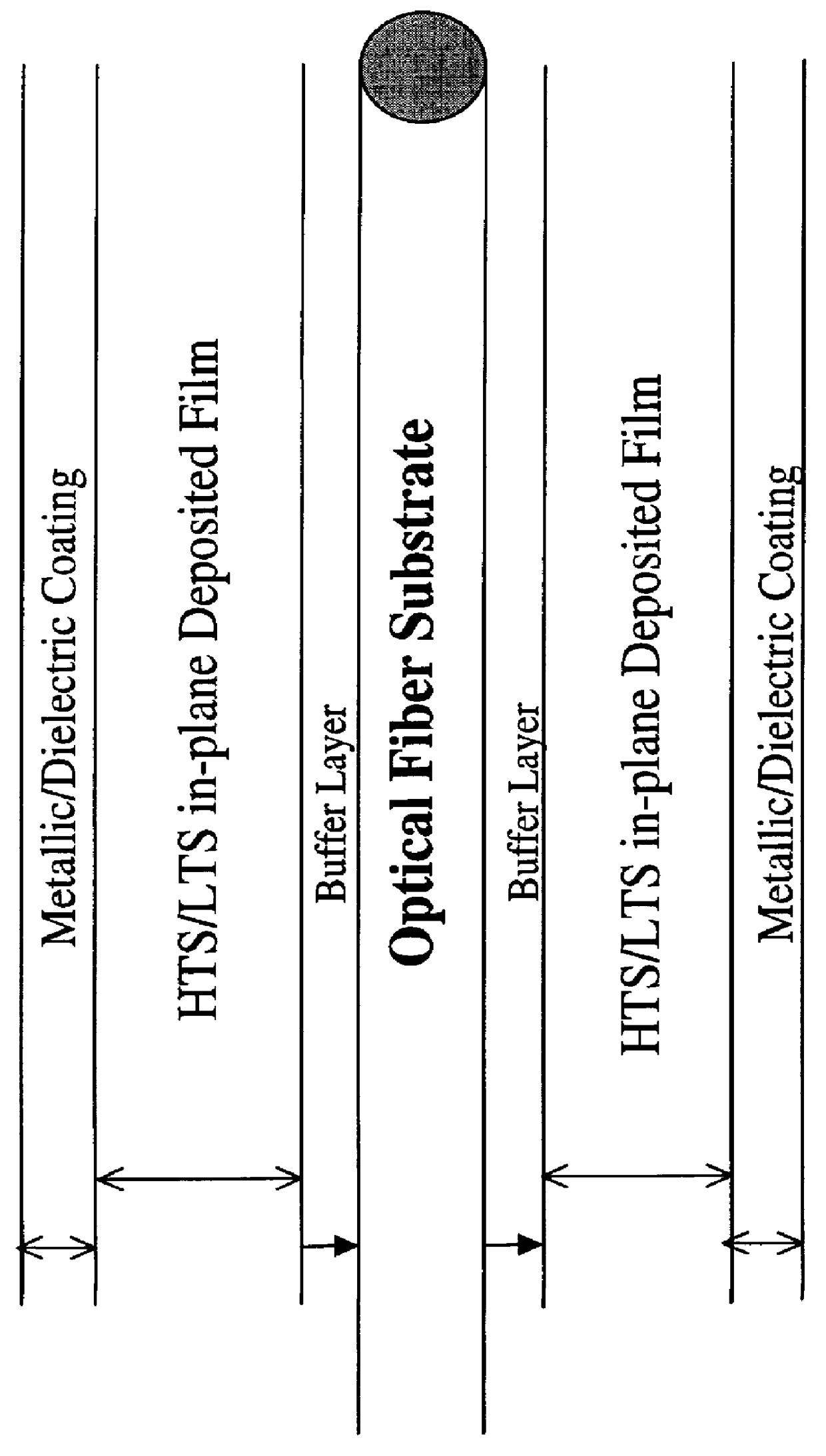
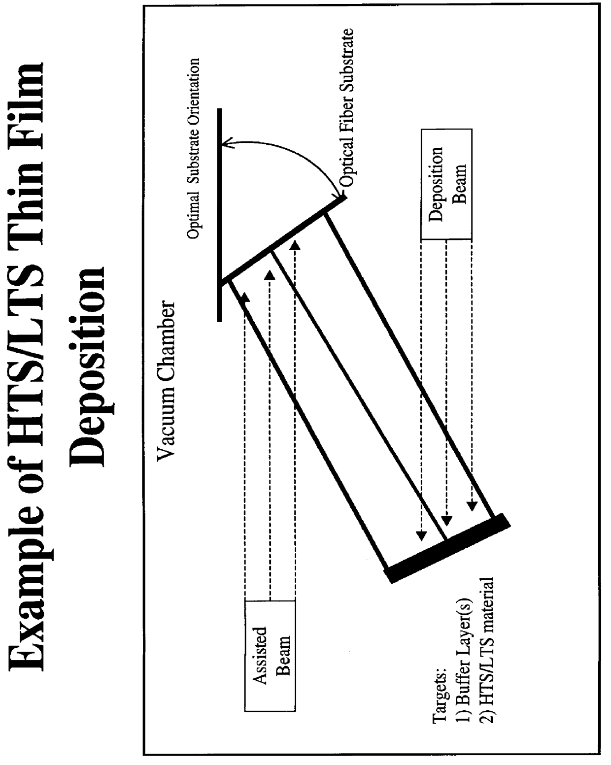
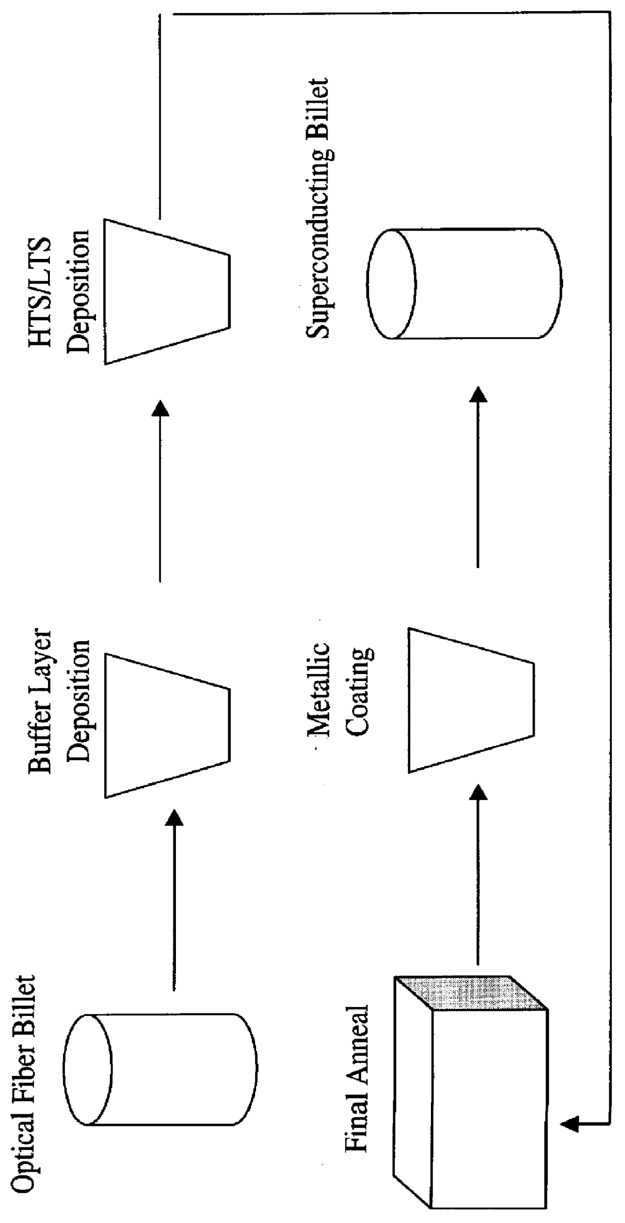
A typical flow chart of the fabrication process of the present invention is illustrated in FIG. 4. The process begins with the introduction of the optical fiber billet 10. The billet consists of fully characterized optical fiber of uniform cross section. In the next step of the process 20, a buffer layer(s) is then deposited in a controlled environment (i.e. temperature, pressure, chemical species present, etc.) on the optical fiber to enhance grain growth. Next 30, the LTS or HTS material is deposited in a controlled environment (i.e. temperature, pressure, chemical species present, etc.). Next, the optical fibers may then undergo a final anneal 40. The last processing step 50, is the introduction of a noble metallic material for electric and thermal stability and / or a dielectric material for electrical insulation and environmental protection. The post-processed wire is then transposed, twisted and cabled 60 into multi-strand conductor. The final step 70 is the installation of the ...


PUM

PropertyMeasurementUnit
Temperatureaaaaaaaaaa
Lattice constantaaaaaaaaaa
Currentaaaaaaaaaa

Abstract

This patent application relates to the use of thin high temperature fibers, specifically optical fibers, for use as a substrate material in the fabrication of long-length low temperature superconducting and high temperature superconducting wire. The superconducting material is deposited on the fiber using either a thin or thick film deposition technique. The fiber can have a dual use in the transmission of data using either traditional optical means or the transmission of electrical current via the deposited superconductor. A buffer layer or layers is used between the high temperature fiber and the superconductor to promote grain alignment and enhance the current carrying capacity of the wire.

Description

BACKGROUND--FIELD OF INVENTIONThis invention relates to the use of a high temperature fiber, specifically an optical fiber, for use as a substrate material in the fabrication of long length low temperature superconducting and high temperature superconducting wire using thin and thick film deposition techniques.BRIEF DESCRIPTION OF FIGURESFIG. 1FIG. 1 shows a typical embodiment of the proposed invention. A noble metallic coating can be deposited to improve the superconducting grain growth as well as improve the electrical and thermal stability of the superconducting wire itself. To further improve the expitaxial growth of the superconducting material and hence improve the current carrying capacity, an appropriate crystalline buffer layer(s) can be deposited on the optical fiber. Finally, an appropriate dielectric coating can be deposited in order to provide electrical insulation and environmental protection.FIG. 2FIG. 2 shows a typical embodiment of a HTS / LTS thin film deposition tec...

Claims


Application Information

Patent Timeline
IPC IPC(8): C23C28/00G02B6/02H01B12/06H01L39/24
CPCC23C28/00G02B6/02G02B6/02395H01L39/2454H01L39/248H01B12/06G02B6/4416Y02E40/642Y02E40/60H10N60/0576H10N60/0801
Inventor REY, CHRISTOPHER M.
Owner REY CHRISTOPHER M
Why Eureka
Try Eureka