Method of filling shallow trenches

Inactive Publication Date: 2001-01-30
CHARTERED SEMICONDUCTOR MANUFACTURING
View PDF8 Cites 175 Cited by
  • Summary
  • Abstract
  • Description
  • Claims
  • Application Information

AI Technical Summary

Problems solved by technology

There are some process problems in the prior art associated with shallow trench isolation (STI) and the integration of trench filling by silicon dioxide films.
Process problems that arise under certain conditions are the formation of voids and seams in the isolating dielectrics employed in the trench fill process.
Unfortunately, aspect ratios exceeding 2:1, and even approaching 4:1, and higher are nee

Method used


Image

  • Method of filling shallow trenches
  • Method of filling shallow trenches
  • Method of filling shallow trenches

Examples


Embodiment Construction

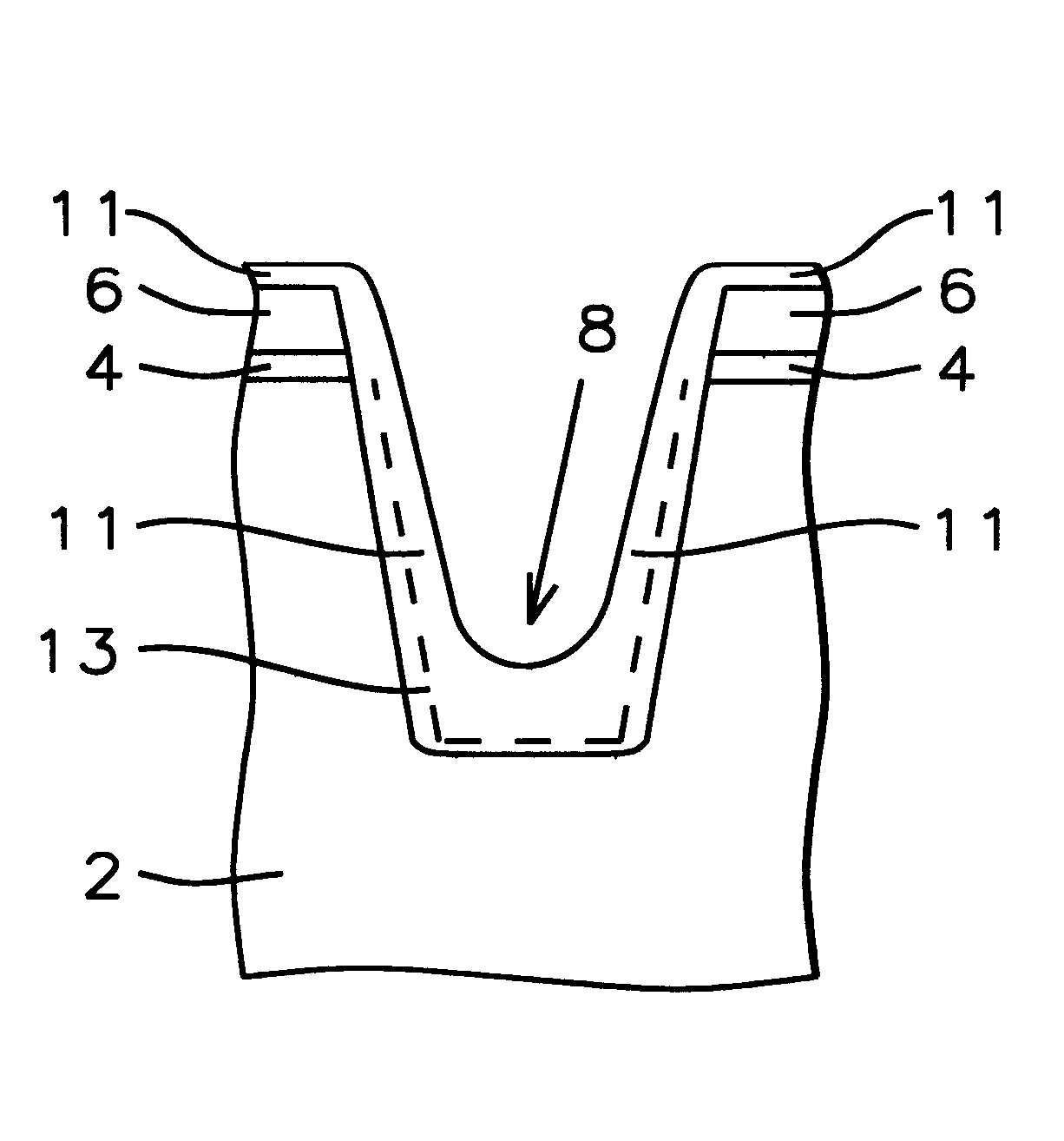
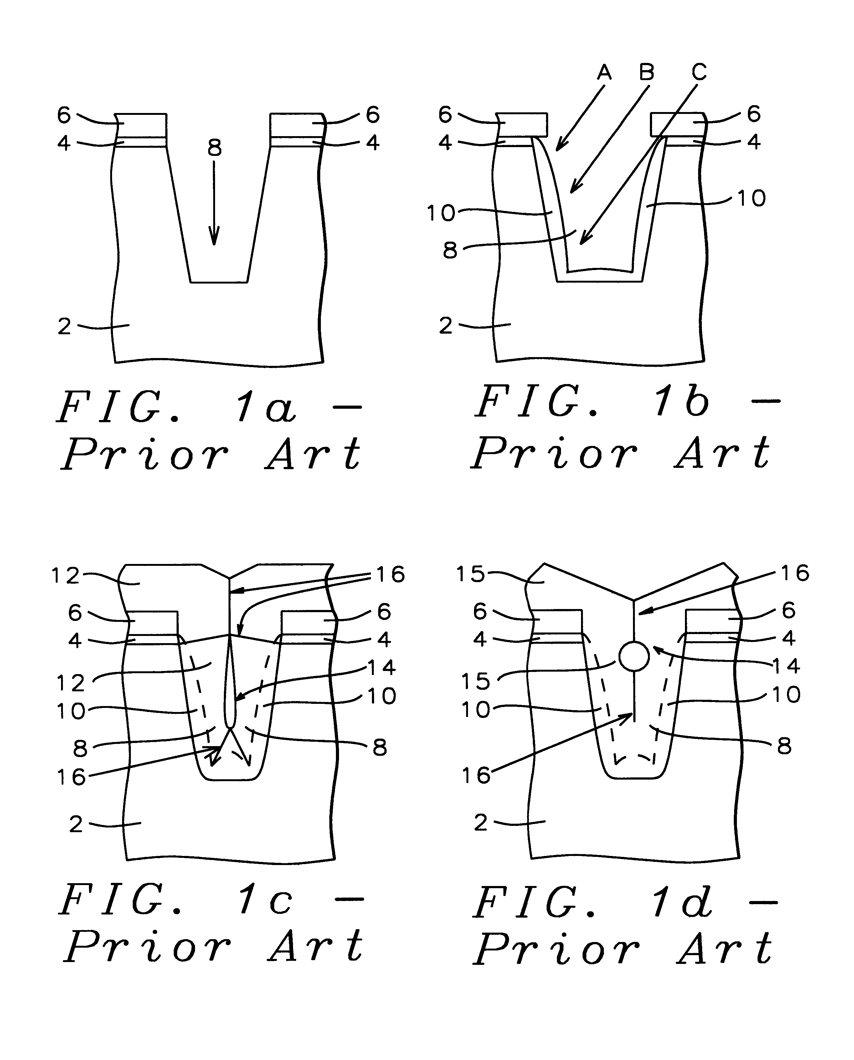
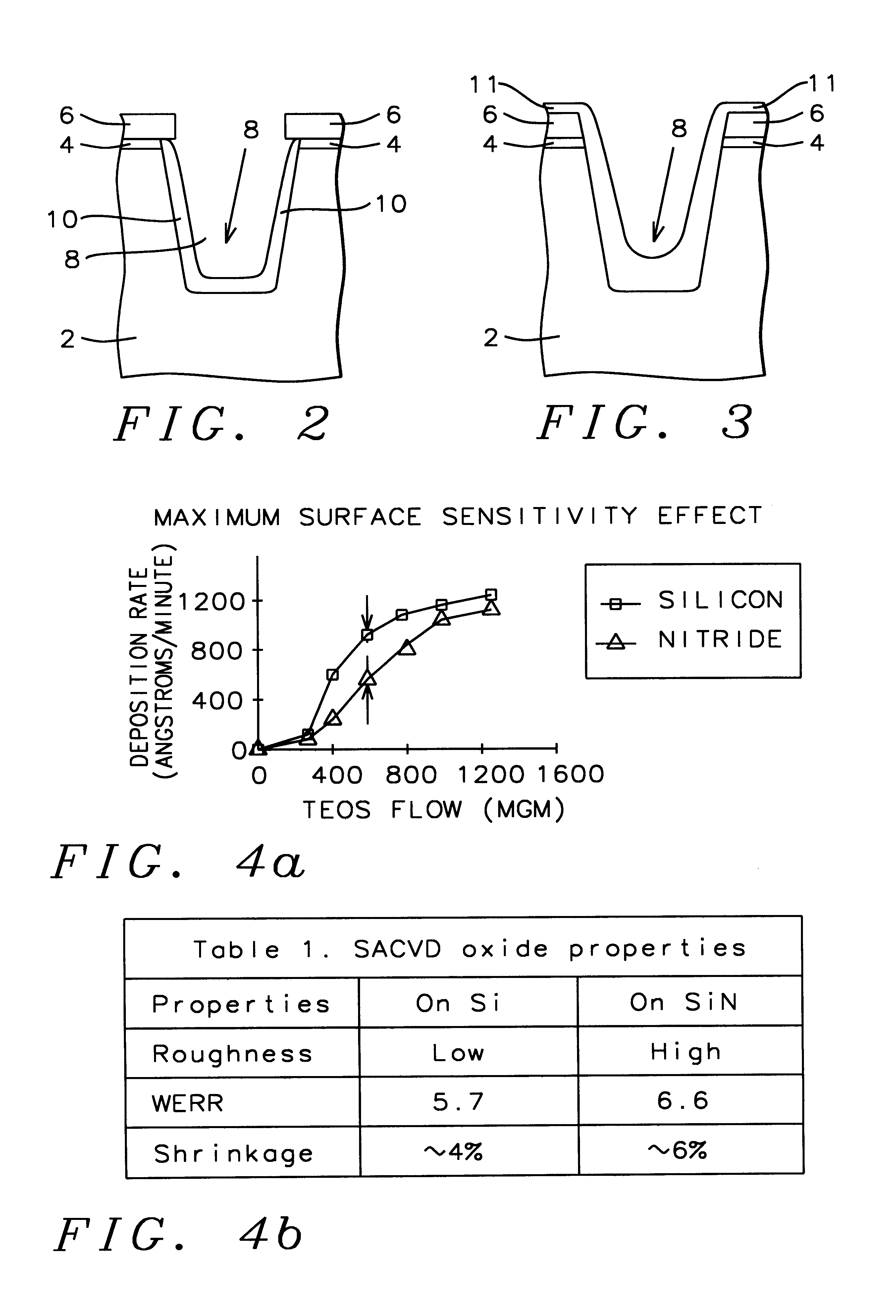
As background to the present invention, a conventional method of fabricating shallow trench isolation (STI) is illustrated as Prior Art in cross-sectional sketches in FIGS. 1a, 1b, 1c, and 1d. As shown in FIG. 1a, the semiconductor substrate 2 is the base starting material for the trench structures. A thermal silicon dioxide pad oxide layer 4 is grown on the silicon substrate, as depicted in FIG. 1a. The thermally grown silicon dioxide pad is grown specifically at a temperature of approximately 1050.degree. C. using an oxygen gas ambient. The thermally grown silicon dioxide pad film thickness is from about 100 to 200 Angstroms. Then a chemically vapor deposited (CVD) silicon nitride layer, pad nitride 6, is deposited on top of the pad silicon dioxide, shown in FIG. 1a. The pad silicon nitride film is deposited, using low pressure chemical vapor deposition (LPCVD ) with the following specific reactor conditions: temperature 700.degree. C., pressure 0.3 Torr, and ratio of ammonia to d...


PUM


Abstract

This invention relates to a method of fabrication used for semiconductor integrated circuit devices, and more specifically to an improved method of filling shallow trenches, in shallow trench isolation, STI sub-quarter micron technology. The present method relates to a process for forming trench gap filling with chemically vapor deposited (CVD) silicon dioxide layers within trenches within substrates employed in integrated circuit fabrication.There is first provided a silicon substrate having a trench formed therein. There is then formed a silicon dioxide layer through tetraethylorthosilicate (TEOS) and ozone reaction, at either sub-atmospheric, or atmospheric pressure, with enhanced surface sensitivity features, which lines the trench providing corner rounding. Then there is a thermal oxidation to form within the trench a thermal silicon dioxide layer underneath the TEOS-ozone trench silicon dioxide liner. Finally, there is formed on top of the trench a silicon dioxide layer formed by either low pressure CVD using TEOS, or non-surface sensitive TEOS ozone CVD, or a high-density plasma CVD process. All layers are further annealed to form a void-free trench fill.

Description

(1) Field of the InventionThis invention relates to a method of fabrication used for semiconductor integrated circuit devices, and more specifically to a method of filling shallow trenches, in shallow trench isolation, STI sub-quarter micron technology. The present method relates to a method for forming of void-free trench gap fill with chemically vapor deposited (CVD) silicon oxide films using a layer of silicon dioxide liner deposited from a TEOS-ozone mixture at atmospheric pressure chemical vapor deposition (APCVD) or at sub-atmospheric pressure thermal chemical vapor deposition (SACVD) conditions, within trenches within substrates employed in integrated circuit fabrication.(2) Description of Prior ArtIntegrated circuits are formed from semiconductor substrates within and upon whose surfaces are formed resistors, transistors, diodes and other electrical circuit elements. The electrical circuits elements are connected internally and externally to the semiconductor substrate upon ...

Claims


Application Information

Patent Timeline
IPC IPC(8): H01L21/70H01L21/762
CPCH01L21/76232
Inventor VASSILIEV, VLADISLAVPEIDOUS, IGOR
Owner CHARTERED SEMICONDUCTOR MANUFACTURING
Why Eureka
Try Eureka