Inductively coupled plasma CVD

a plasma cvd and inductive coupling technology, applied in the field of inductive coupling plasma cvd, can solve the problems of high cost, complex ecr and helicon sources which rely on magnetic fields, and unsuitable techniques for gap widths below 0.5 microns,

Inactive Publication Date: 2001-02-06
LAM RES CORP
View PDF77 Cites 196 Cited by
  • Summary
  • Abstract
  • Description
  • Claims
  • Application Information

AI Technical Summary

Problems solved by technology

That single step process replaced sequential gap-filling and planarization steps wherein CVD SiO.sub.2 was subjected to plasma etch-back steps, such technique being unsuitable for gap widths below 0.5 microns and aspect ratios (gap height:width) above 1.5:1.
Prior art apparatuses suffer from several serious disadvantages with respect to IMD applications.
ECR and helicon sources which rely on magnetic fields are complex and expensive.
Moreover, magnetic fields have been implicated to cause damage to semiconductor devices on the wafer.
ECR, helicon and helical resonator sources also generate plasmas remotely from the wafer, making it very difficult to produce uniform and high quality films at the same time and also

Method used


Image

  • Inductively coupled plasma CVD
  • Inductively coupled plasma CVD

Examples


example i

(Gap-filling process)

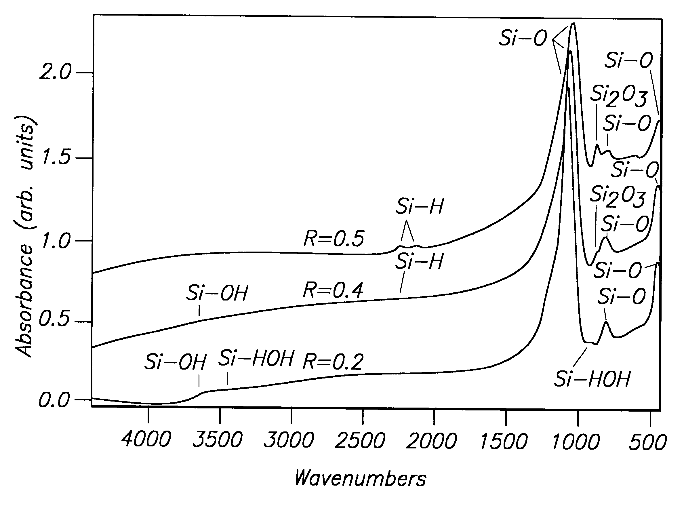
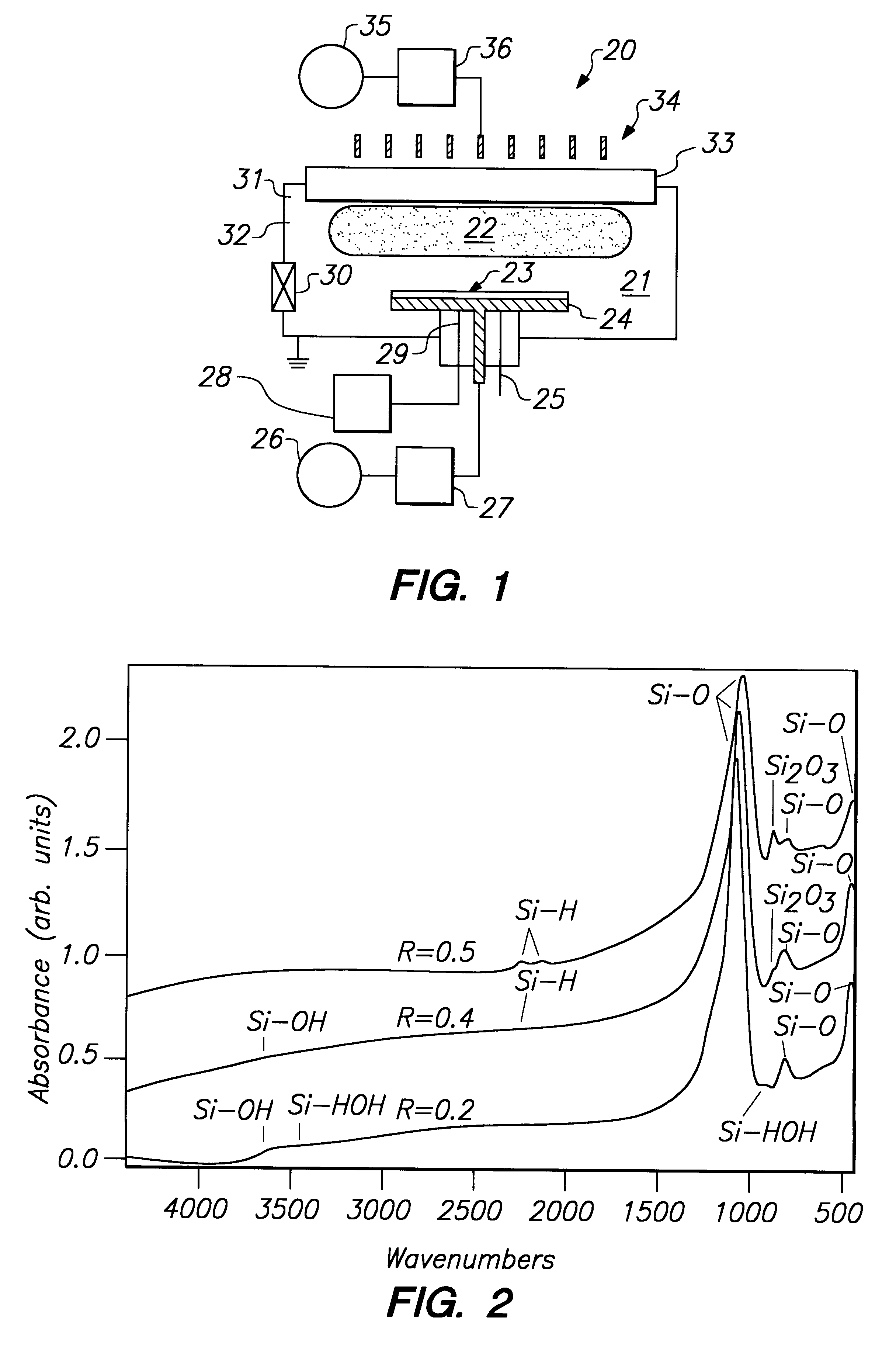
SiO.sub.2 IMD depositions were conducted in an ICP system similar to that of FIG. 1. Mechanically-clamped 150 mm wafers were employed. Two gas rings located at the bottom edge of window 33 were employed. One ring distributed the SiH.sub.4 and the other distributed the Ar and O.sub.2. System parameters are set forth in Table 1. The electrode temperature was maintained at 80.degree. C.

Effect of Oxygen to Silane Mass Flow Ratio (at constant total flow) on Film Properties

The film stoichiometry was determined by the chemical composition of the plasma, established primarily by the ratio R of the silane and oxygen mass flow rates: R=Q.sub.SiH4 / (Q.sub.SiH4 +Q.sub.O2) where Q is the gas mass flow rate. Note that the effective oxygen-silane ratio that the wafer sees also depended on other process parameters. The effect of R on the film properties is shown in Table 2.

The plasma chemistry for the deposition can be broadly classified into the following reactions:

R<0.5: SiH....

example ii

(GaM-fill and Capping Processes)

SiO.sub.2 IMD and capping depositions were conducted in an ICP system similar to that of FIG. 4. In this example 200 mm wafers were processed. The wafers were electrostatically clamped to a thermally controlled chuck. The lower electrode was powered by a 13.56 MHz generator. A 2000 l / sec pump to improve the pumping speed at high flows was also implemented into the ICP / CVD system. ICP power ranging from 1000 to 2500 watts was used. High bias power was used for the gap fill process and ranged from 500 to 2500 watts.

Typical process parameters are shown in Table 5 for the gapfill, cap, and sacrificial cap layers and the corresponding film characteristics. The table also lists the preferred ranges for the process parameters.

In these depositions (0.5 .mu.m gaps), argon was included in the process gas. However, the addition of argon is not always necessary as indicated in the preferred ranges. In the deposition of the cap layer, the initial deposition can em...


PUM

PropertyMeasurementUnit
Pressureaaaaaaaaaa
Pressureaaaaaaaaaa
Angleaaaaaaaaaa

Abstract

A method of depositing a dielectric film on a substrate in a process chamber of an inductively coupled plasma-enhanced chemical vapor deposition reactor. Gap filling between electrically conductive lines on a semiconductor substrate and depositing a cap layer are achieved. Films having significantly improved physical characteristics including reduced film stress are produced by heating the substrate holder on which the substrate is positioned in the process chamber.

Description

The present invention relates to a method and apparatus for high-density plasma-enhanced chemical vapor deposition of semiconducting and dielectric films and more particularly to techniques for depositing such films into high aspect ratio gaps on semiconductor substrates such as silicon wafers having metal interconnection layers.DESCRIPTION OF THE RELATED ARTChemical vapor deposition (CVD) is conventionally used to form various thin films in a semiconductor integrated circuit. CVD can form thin films such as SiO.sub.2, Si.sub.3 N.sub.4, Si or the like with high purity and high quality. In the reaction process of forming a thin film, a reaction vessel in which semiconductor substrates are arranged can be heated to a high temperature condition of 500 to 1000.degree. C. Raw material to be deposited can be supplied through the vessel in the form of gaseous constituents so that gaseous molecules are thermally dissociated and combined in the gas and on a surface of the substrates so as to...

Claims


Application Information

Patent Timeline
IPC IPC(8): C23C16/507C23C16/40C23C16/50H01L21/70H01L21/768H01L21/02H01L21/316
CPCC23C16/402C23C16/507H01J37/321H01L21/02126H01L21/02164H01L21/02211H01L21/02274H01L21/02301H01L21/02315H01L21/02362H01L21/31612H01L21/76837Y10S438/906Y10S438/902C23C16/40
Inventor SHUFFLEBOTHAM, PAUL KEVINMCMILLIN, BRIANDEMOS, ALEXNGUYEN, HUONGBERNEY, BUTCHBEN-DOR, MONIQUE
Owner LAM RES CORP
Why Eureka
Try Eureka