

Impedance matching circuit, high speed semiconductor integrated circuit employing the same and computer system employing the integrated circuit
- Summary
- Abstract
- Description
- Claims
- Application Information
AI Technical Summary
Problems solved by technology
Method used
Image

Examples
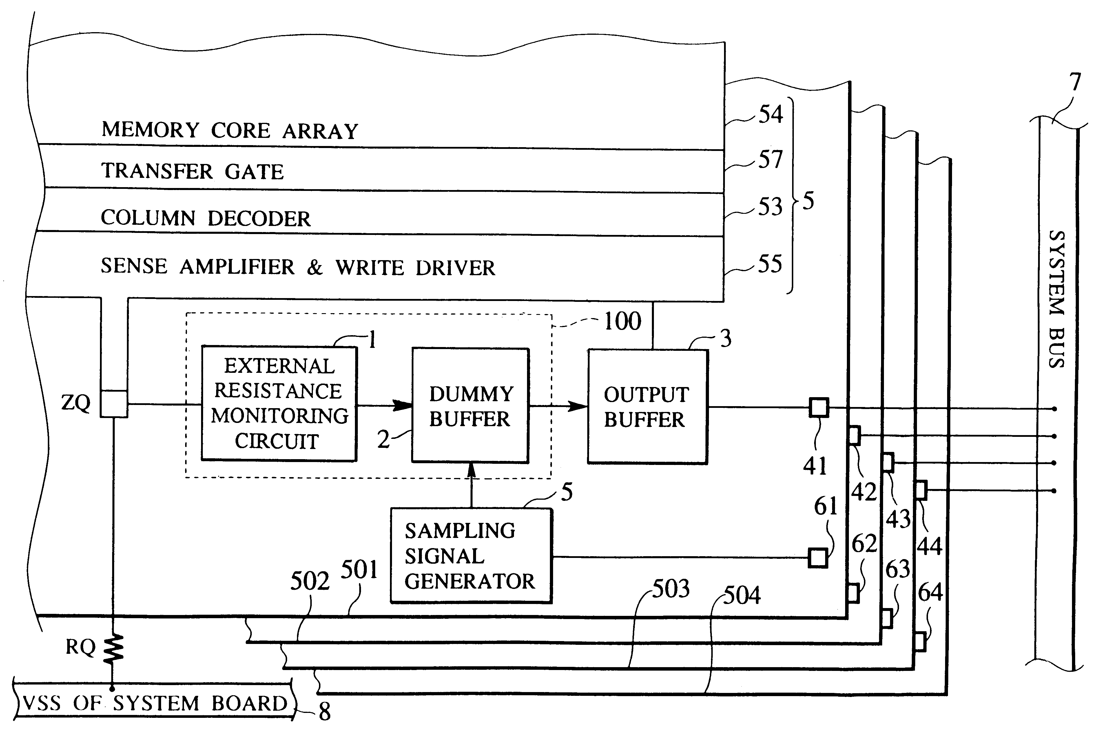
first embodiment
The first embodiment is capable of controlling an impedance matching error of the output buffer 3 within the range of .+-.10% when the resistance value of the external resistor RQ is, for example, 175.OMEGA..ltoreq.RQ.ltoreq.352.OMEGA., thereby securing required product specifications. This improves a margin for circuit errors, simplifies the structure of the impedance matching circuit, and reduces the occupation area of the impedance matching circuit. Then the utilization efficiency of the real estate (or the chip area) improves, and the integration density of the LSI chip can be increased.
The comparator 32 may compare a voltage applied to the dummy buffer 2 with the reference voltage provided from the node between the resistors R1 and R2, and according to a comparison result, the control circuit 31 may match the impedance of the dummy buffer 2 with the impedance of the external resistor RQ. This configuration provides the same effect as the first embodiment mentioned above.
second embodiment
(SECOND EMBODIMENT)
As explained above, the first embodiment determines the impedance of the external resistor RQ from a detected current I.sub.ZQ passing through the external resistor RQ. According to the detected current I.sub.ZQ, the first embodiment controls set of data bits D.sub.1 to D.sub.N applied to the set of nMOS transistors T.sub.1 to T.sub.N of the dummy buffer 2 so that a supply voltage applied to the MOS transistors T.sub.1 to T.sub.N is equalized to the voltage VZQ of the ZQ-terminal, thereby matching the impedance of the dummy buffer 2 with the impedance of the external resistor RQ. Namely, to the set of data bits D.sub.1 to D.sub.N determines the combined impedance of the pull-down output buffer 3. The combined impedance of the output buffer 3 is set to be "a" times the combined impedance of the dummy buffer 2 where "a" is a constant. Since the set of bias conditions of respective transistors in the dummy buffer 2 is identical to that of the output buffer 3, the buf...
second embodiments
The first and second embodiments of FIGS. 6 and 9 employ the second high level supply voltage VDD, which is the power supply for general circuits including the peripheral circuits and the internal circuit such as the memory core, as the high level voltage source for the current mirror circuits. Instead of the second high level supply voltage VDD, the current mirror circuits may use the first high level supply voltage VDDQ. In this case, the circuit for detecting the current I.sub.ZQ passing through the external resistor RQ and the output buffers use the same voltage source. As a result, noise in the first high level supply voltage VDDQ appears both in the matching circuits and output buffers, to prevent a deterioration of matching accuracy. Therefore, it is always possible to correctly match the impedance of the output buffer 3 with the impedance of the external resistor RQ.
The comparators 32 and 34 of FIG. 9 may compare voltages applied to the dummy buffers 2D and 2U with the refer...
PUM
 Abstract
Description
Claims
Application Information