
Apparatus for mounting an electronic component

a technology for mounting apparatus and electronic components, applied in the direction of manufacturing tools, transportation and packaging, packaging, etc., can solve the problems of reducing production efficiency, forming air bubbles, and shortened time, and achieves shortening production time, reducing production costs, and improving production efficiency

Inactive Publication Date: 2001-03-27
PANASONIC CORP
View PDF22 Cites 11 Cited by
  • Summary
  • Abstract
  • Description
  • Claims
  • Application Information

AI Technical Summary

Benefits of technology

According to a fifth aspect of the present invention, in the fourth aspect, the sealant in the first application process has heat cycle function and moisture resistance and resists being mingled with air bubbles, while the sealant in the second application process smoothly fits to a bump of an electrode part of the electronic component, and has good fluidity and low surface tension.
According to an 11th aspect of the present invention, in the 10th aspect, the sealant used by the first applying device has heat cycle function and moisture resistance and resists being mingled with air bubbles, while the sealant used by the second applying device smoothly fits to a bump of an electrode part of the electronic component, and has good fluidity and low surface tension.
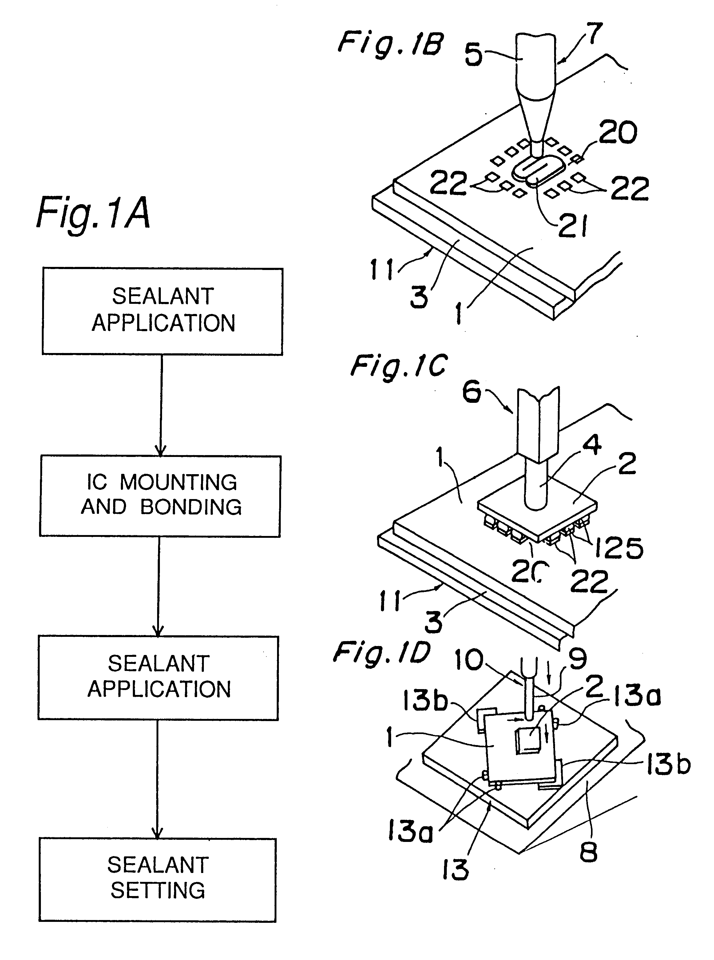
In the first aspect of the present invention, the electronic component is arranged at the position of the object to which the electronic component is to be mounted and where the sealant is applied beforehand in the first application process. The sealant is quickly, sufficiently and forcibly applied in the first application process simply by avoiding the electrode at the arrangement position, to be in tight contact with the arranged electronic component and the object, and then, without causing any obstruction to a successive bonding of electrodes of the electronic component and the object, the bonding of the electrodes is performed usually. In the second application process, the sealant is applied to the periphery of the electronic component in the same manner as conventionally, which is enough to send a sealant to the sealant applied beforehand under the electronic component. The second application process is accordingly conducted speedily and sufficiently. Air bubbles are hard to mingle with the sealant between the electronic component and the object, whereby mounting failures due to breakage or corrosion of the electronic component because of the air bubbles can be reduced. The sealant is applied each time in a short time although applied twice, so that a production time is shortened and production efficiency is improved. The first application process serves to bond the electronic component arranged thereafter to the circuit board, and therefore the electronic component is prevented from being displaced after the arrangement. Moreover, the electronic component is bonded and sealed with improved performance, whereby a yield and product quality are enhanced.
In the second and eighth aspects of the present invention, an application locus and a movement speed in the writing method can be set freely, thereby to easily cope with any arrangement of electrodes on the object. Moreover, any required application density and application amount are satisfied with ease. Particularly, the writing method utilized in the first application is effective to reduce mounting failures furthermore. Since an application position of the sealant is correctly controlled, even the sealant of low viscosity does not flow to the electrodes and thus does not hinder the bonding of electrodes once a safe gap is properly secured to the electrodes. The low viscous sealant improves working efficiency further owing to its good fluidity.
In the third and ninth aspects of the present invention, any arrangement of electrodes on the object is coped with by the print pattern set beforehand to a screen, and a required application density is ensured, whereby mounting failures are decreased furthermore. The sealant can be applied instantaneously simply by opening / closing the screen and moving a squeegee to a plurality of electronic component arrangement positions at one time. Working efficiency is improved furthermore.
The fourth-sixth and 10th-12th aspects of the present invention can cope well with different application conditions such as different application methods, different instruments, etc. between the first and second application processes. Thus, each of the first and second applications can be performed well.

Problems solved by technology

The conventional method as above finds difficulty in flowing the sealant i to the lower portion of the electronic component b, because a gap between a lower face of the electronic component b and the circuit board d is as narrow as several tens .mu.m, and moreover the sealant i is highly viscous.
A feed time for the flow of sealant i is consequently apt to be lengthy, in other words, production time is lengthened thereby lowering production efficiency.
Besides, the sealant i fed to the gap tends to be insufficient in feed amount, resulting in the formation of air bubbles which are to be enclosed.
A pressure increase or decrease due to the expansion / shrinkage of air bubbles sometimes invites breaks of the electronic component b or the humidity in the air bubbles causes corrosion of the electrode or the like, thus leading to mounting faults.

Method used


Image

  • Apparatus for mounting an electronic component
  • Apparatus for mounting an electronic component
  • Apparatus for mounting an electronic component

Examples


first embodiment

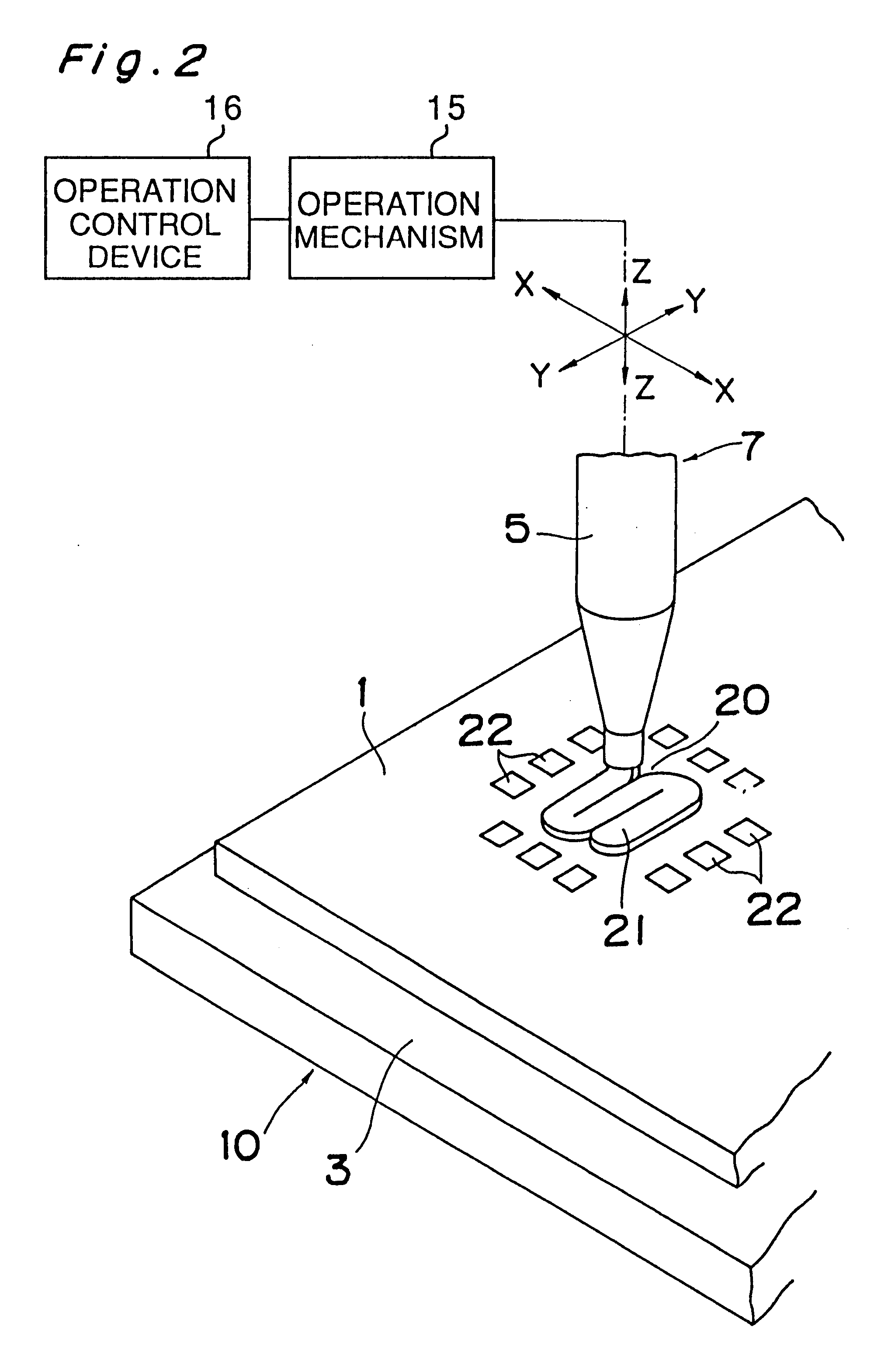
FIGS. 1 through 7 show a mounting method and a mounting apparatus according to a first embodiment of the present invention. As indicated in FIGS. 1B-1D, the first embodiment is related to mounting of an electronic component 2 to an object, e.g., a circuit board 1 on which the component is to be mounted. A mounting apparatus for the component 2 which comprises a positioning base 3 as a holding device 11 as shown in FIGS. 1B, 1C, 2, 3 for positioning and holding the circuit board 1, a bonding device using, for example, a suction nozzle 4 as shown in FIG. 1C as a bonding device 6 for arranging and bonding the electronic component 2 onto the circuit board 1, and a first sealant applying device 7 having a dispenser 5 arranged so as to be movable over the circuit board 1 in three dimensions as shown in FIGS. 1B, 2. Although it is satisfactory to position the bonding device 6 and the first applying device 7 at the same stage of the same machine, these devices may be positioned at different...

second embodiment

FIG. 8 shows a dispenser 5 which is particularly suitable for a first application process in a mounting method and a mounting apparatus according to a second embodiment of the present invention. The dispenser 5 has a plurality of discharge openings 5a for the sealant 21. In the second embodiment, three discharge openings 5 are provided and arranged in one row. However, the present invention is not restricted to this arrangement and a proper number of the discharge openings may be arranged in any manner.

The discharge openings 5a are connected to solenoid valves 33a, 33b, 33c by joints 31 and air tubes 32 respectively. Reference numerals 34, 35 in FIG. 8 indicate a cap of the dispenser 5 and an air leak prevention seal, respectively. The solenoid valves 33a, 33b, 33c are connected to regulators 36a, 36b, 36c, respectively. Each of the regulators 36a, 36b, 36c can regulate the pressure of air supplied from a compressor 201. Therefore, the discharge amount of the sealant 21 from each di...

third embodiment

FIG. 9 indicates a screen printing device for carrying out a first application process in a mounting method and a mounting apparatus according to a third embodiment of the present invention.

This operation will be described. The circuit board 1 is held on a stage 41 serving as the holding device. A screen 43 patterned by an emulsion 42 is positioned so as to agree with a wiring pattern of the board 1. The sealant 21 is placed on the screen 43. The sealant 21 is applied on the circuit board 1 by moving a squeegee 44 held in pressed contact with the screen 43. The above is the same as a general method of screen printing. Nearly the same operation and effect as achieved in the first embodiment are realized in the first application process.

In comparison with the writing method whereby the sealant 21 is applied flat in the breadthwise direction, an edge of the pattern of the emulsion 42 formed on the screen 43 is sharpened and is easily separated from the screen. The third embodiment can ...


PUM

PropertyMeasurementUnit
Timeaaaaaaaaaa
Thicknessaaaaaaaaaa
Pressureaaaaaaaaaa

Abstract

A method of and apparatus for mounting an electronic component at a specified position of an object. The method includes applying a sealant in a first application process. The sealant is quickly, sufficiently and forcibly applied in the first application process simply by avoiding electrodes at the arrangement position, and tightly contacting the arranged electronic component and the object. Then the bonding of the electrodes is performed in the usual manner. A second application process is carried out by applying a sealant to the periphery of the electronic component in the same manner as in the convention method, which is sufficient to cause the sealant to flow to the sealant previously applied under the electronic component. The second application process can be accordingly conducted speedily and sufficiently. Air bubbles will not be trapped between the electronic component and the object, with the result that mounting failures due to breakage or corrosion of the electronic component can be reduced. Only a short period of time is required to apply the sealant even though it is applied twice, so that production time is shortened and production efficiency is improved.

Description

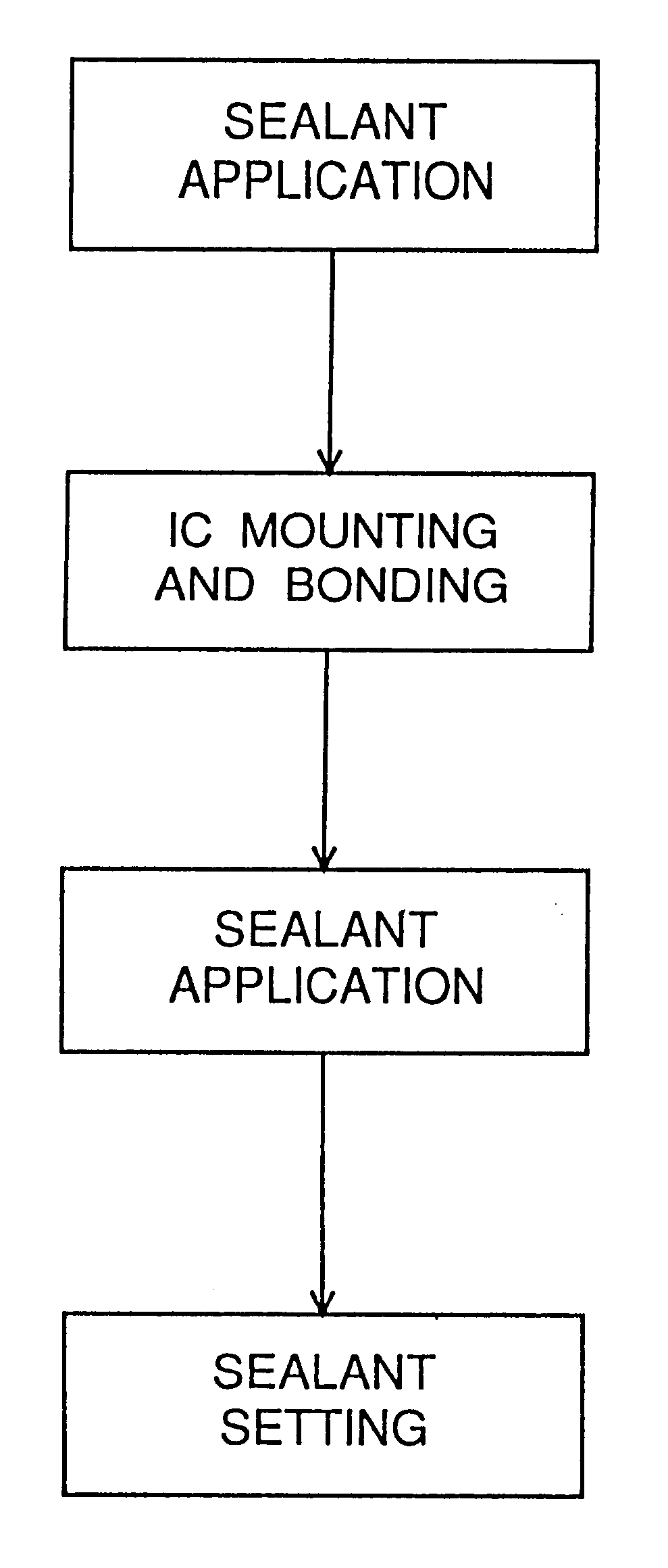
The present invention relates to a method for mounting an electronic component by means of arranging and sealing of the electronic component on an object such as a circuit board to which the component is mounted and, an apparatus and a dispenser used in the method.A technique called as COB (CHIP ON BOARD) has attracted attention in recent years, as a way of mounting electronic components on a circuit board, in which electronic components are mounted onto electrodes on a circuit board in a state of the electronic components faced downward. The COB technique will be described with reference to the drawings.FIG. 10A is a flow chart of the conventional COB method. Based on this figure, the description is made. Referring first to FIG. 10B, according to the conventional COB method, an electronic component b is first arranged and bonded to a circuit board d. Electrode parts c as shown in FIG. 10B are provided on the circuit board d for the electric connection to the electronic component b....

Claims


Application Information

Patent Timeline
IPC IPC(8): H01L21/02H01L21/56H05K13/04H01L21/52H01L21/60
CPCH01L21/563H05K13/0465H05K13/0469H01L24/29H01L24/743H01L24/27Y10T29/53174H01L2224/16225H01L2224/73203H01L2224/83192H01L2224/83194H01L2924/01004H01L2924/01005H01L2924/01033H01L2924/01039H01L2924/01047H01L2924/01082H01L2924/01006Y10T156/17Y10T156/1798Y10T29/53178H01L2224/743H01L2924/3512H01L2924/00H01L2224/11005H01L2224/75611H01L21/50
Inventor IMANISHI, MAKOTOKABESHITA, AKIRAENCHI, KOHEISHIDA, SATOSHI
Owner PANASONIC CORP
Learn More