Process for the production of semiconductor device

a semiconductor and production process technology, applied in the direction of semiconductor devices, electrical appliances, transistors, etc., can solve the problems of difficult to form a uniform semiconductive layer having difficult to form a semiconductive layer with a particularly thin thickness, and large critical dimension loss, so as to reduce the operation speed of the semiconductor device

Inactive Publication Date: 2001-04-10
SONY CORP
View PDF2 Cites 8 Cited by
  • Summary
  • Abstract
  • Description
  • Claims
  • Application Information

AI Technical Summary

Benefits of technology

It is therefore a first object of the present invention to provide a process for the production of a semiconductor device having a structure in which one gate electrode is formed above a channel-forming region, the other gate electrode is formed below the channel-forming region, word lines which are extending portions from the gate electrodes face each other through an insulating film, and the above process can overcome the problem that parasitic capacitance in a portion where the word lines faces each other increases so that the operation speed of the semiconductor device decreases.

Problems solved by technology

That is, the SIMOX method is excellent in uniformity of the SOI layer, while it has a defect that flatness of an interface between an insulating layer and a semiconductive layer is not so good.
The substrate-bonding method shows excellent flatness of an interface between an insulating layer and a semiconductive layer, while it has a defect that it is difficult to form a uniform semiconductive layer having a particularly thin thickness.
However, there is a problem that a critical dimension loss is large when the above oxide layer is formed.
Further, there is another problem that the eventual semiconductive layer is liable to have defects since the semiconductive layer has a stress due to the formation of the oxide layer.
The SOI type semiconductor device is being employed for LSIs of a next generation and generations thereafter, while it is a serious problem that the critical dimension loss is large.
Further, thickness of the semiconductive layer is determined depending upon the thickness of the oxide layer, and it is difficult in many cases to form a semiconductive layer having a thin thickness.

Method used


Image

  • Process for the production of semiconductor device
  • Process for the production of semiconductor device
  • Process for the production of semiconductor device

Examples


example 1

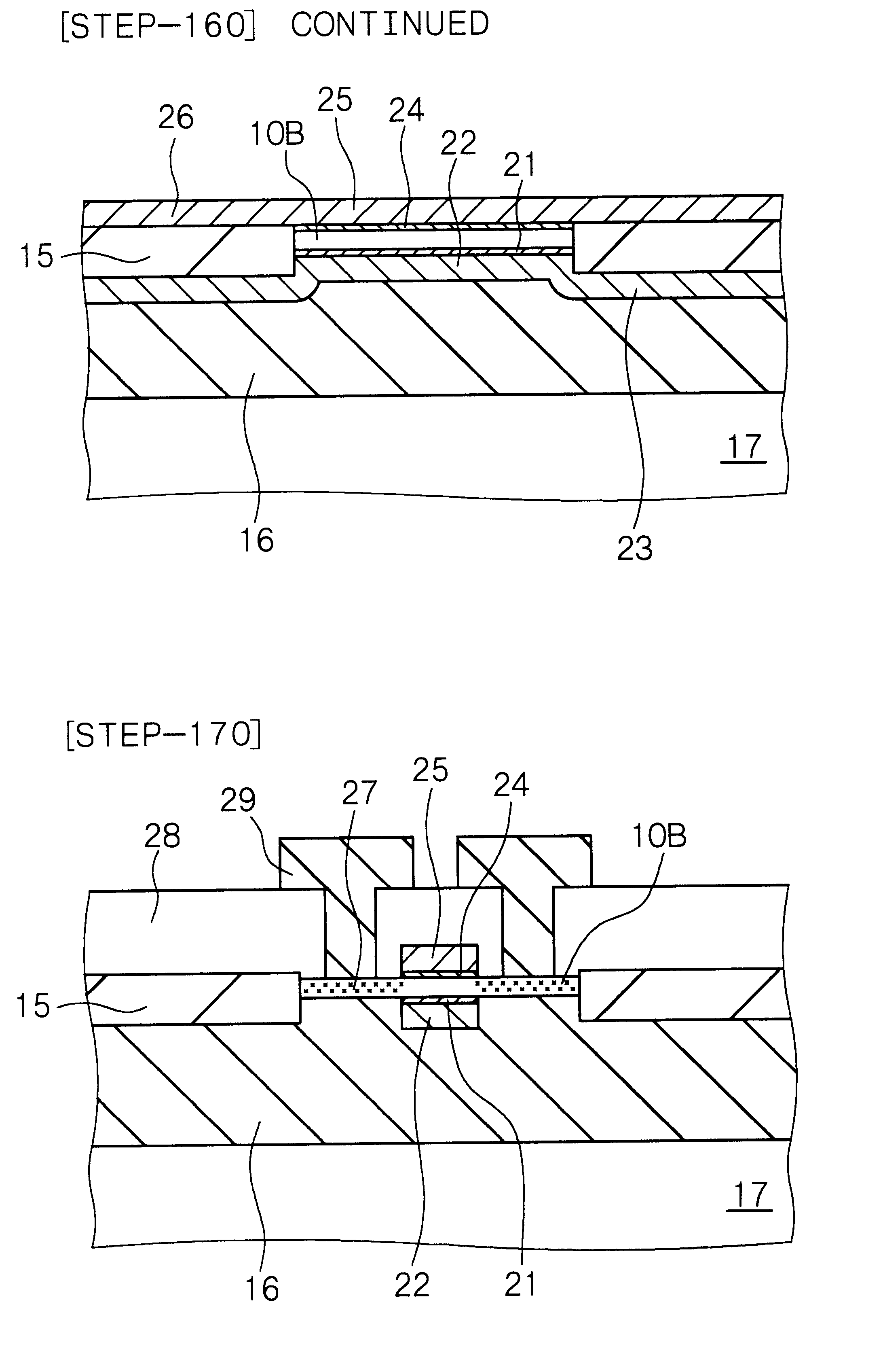
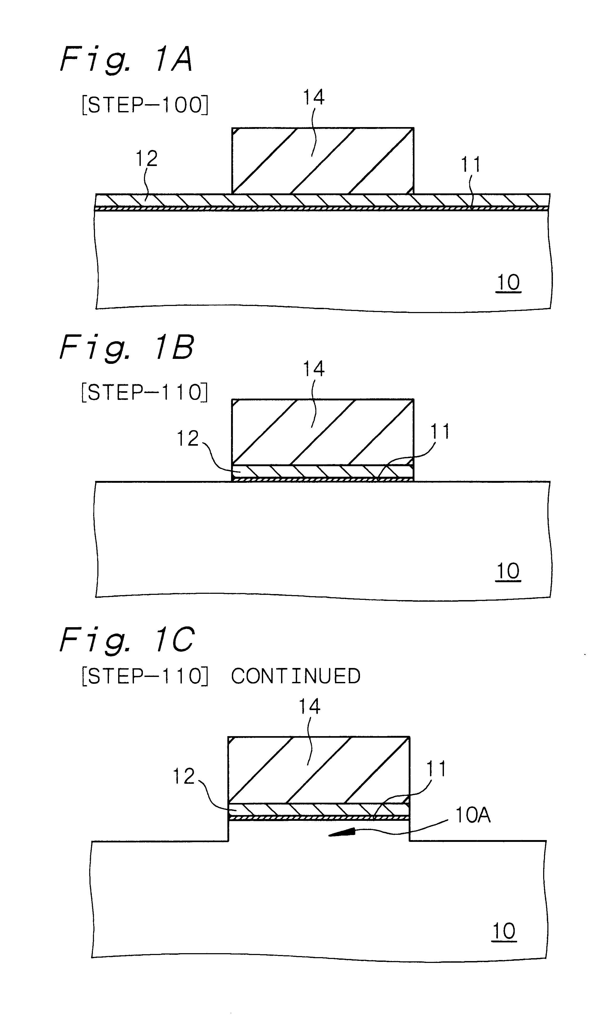
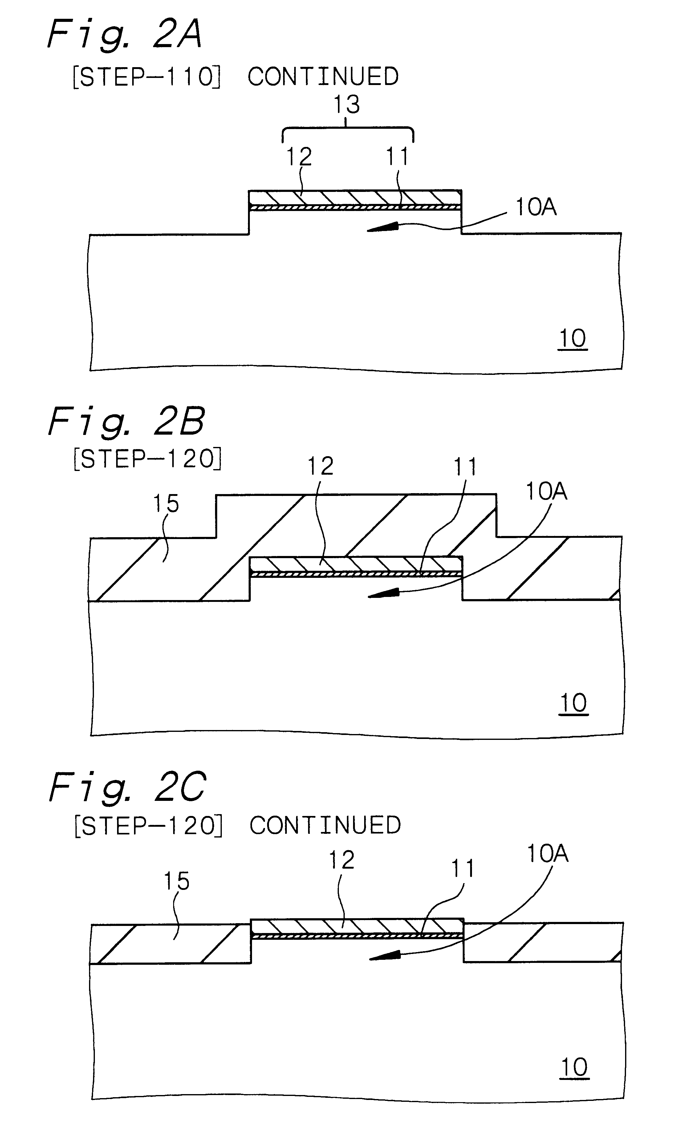
is concerned with a process for the production of a semiconductor device according to the first aspect of the present invention. That is, the process includes the steps of etching a semiconductor substrate to form a convex portion and a concave portion in the semiconductor substrate and filling the concave portion with an insulating film. The process for the production of a semiconductor device in Example 1 will be explained with reference to the steps shown in FIGS. 1A, 1B, 1C, 2A, 2B, 2C, 3A, 3B, 3C, 4A, 4B, 5A, 5B, 6A and 6B showing schematic partial cross-sectional views of a semiconductor substrate, hereinafter. In addition, FIGS. 1A, 1B, 1C, 2A, 2B, 2C, 3A, 3B, 3C, 4A, 4B, 5A, 5B and 6A are schematic partial cross-sectional views of a semiconductor substrate, taken by cutting them along the length direction of a gate electrode, and FIG. 6B is a schematic partial cross-sectional view of the semiconductor substrate, taken by cutting them along the width direction of a gate elect...

example 2

Example 2 is concerned with a process for the production of a semiconductor device according to the second aspect of the present invention. That is, the process includes the steps of etching a semiconductor substrate to form a convex portion and a concave portion in the semiconductor substrate and forming an oxide layer in the concave portion by a selective oxidation method (LOCOS method). The process for the production of a semiconductor device in Example 2 will be explained with reference to the steps respectively shown in FIGS. 7A, 7B, 8A, 8B, 9A, 9B, 10A, 10B and 11 showing schematic partial cross-sectional views of a semiconductor substrate, hereinafter. In addition, FIGS. 7A, 7B, 8A, 8B, 9A, 9B, 10A, 10B and 11 are schematic partial cross-sectional views of a semiconductor substrate, taken by cutting them along the length direction of a gate electrode.

[Step-200]

First, a patterned layer 13 is formed on the surface of a semiconductor substrate 10 composed of a silicon semiconduc...


PUM


Abstract

A process for the production of a semiconductor device comprising the steps of; (a) forming a patterned mask layer on a surface of a semiconductor substrate, (b) etching the semiconductor substrate using the mask layer as an etching mask, to form a step between a portion of the semiconductor substrate covered with the mask layer and an etched portion of the semiconductor substrate, (c) forming an insulating film on the entire surface, and then planarizing the insulating film to cover the etched portion of the semiconductor substrate with the insulating film, (d) removing the mask layer, then, forming a first gate insulating film on an exposed surface of the semiconductor substrate, then forming a first gate electrode on the first gate insulating film, and at the same time, forming a first word line extending from the first gate electrode on the insulating film, (e) forming an interlayer on the entire surface, and bonding the semiconductor substrate and a supporting substrate to each other through the interlayer, (f) grinding and polishing the semiconductor substrate from its rear surface to expose a bottom surface of the insulating film and to leave a semiconductive layer which is the semiconductor substrate remaining after the polishing, surrounded by the insulating film, and (g) forming a second gate insulating film on an exposed surface of the semiconductive layer, then forming a second gate electrode on the second gate insulating film, and at the same time, forming a second word line extending from the second gate electrode on the insulating film.

Description

BACKGROUND OF THE INVENTION AND RELATED ART STATEMENTThe present invention relates to a process for the production of a semiconductor device, and more specifically to a process for the production of a semiconductor device having a structure in which one gate electrode is formed above a channel-forming region and the other gate electrode is formed below the channel-forming region.It is known that complete isolation of semiconductor devices can be achieved and "soft error" and a "latch-up" phenomenon which is inherent in CMOS transistors can be prevented by the formation of a semiconductor device in a semiconductive layer formed on an insulating layer. A semiconductor device formed in a semiconductive layer (to be called an "SOI" layer for convenience hereinafter) formed on an insulting layer will be referred to as an SOI (Silicon-On-Insulator) type semiconductor device. It has been studied since a relatively earlier time whether or not high-speed performance and high reliability of a...

Claims


Application Information

Patent Timeline
Patent Type & Authority Patents(United States)
IPC IPC(8): H01L21/336H01L21/02H01L21/70H01L29/66H01L21/762H01L29/786H01L21/84H01L21/3205H01L27/12
CPCH01L21/76264H01L29/66772H01L29/78648H01L21/76275H01L21/76281H01L21/76283H01L21/3205
Inventor KOMATSU, HIROSHI
Owner SONY CORP
Why Eureka
Try Eureka