Methylated oxide-type dielectric as a replacement for SiO2 hardmasks used in polymeric low K, dual damascene interconnect integration

a technology of methylated oxide and dielectric, which is applied in the direction of basic electric elements, electrical apparatus, semiconductor/solid-state device manufacturing, etc., can solve the problems of increasing device speed, affecting subsequent wafer processing, and conventional usg hardmasks not adhering well

Inactive Publication Date: 2001-04-17
NAT SEMICON CORP
View PDF4 Cites 39 Cited by
  • Summary
  • Abstract
  • Description
  • Claims
  • Application Information

AI Technical Summary

Problems solved by technology

A reduction of the interconnect capacitance decreases RC and in turn, delay, thereby in creasing device speed.
In addition, c

Method used


Image

  • Methylated oxide-type dielectric as a replacement for SiO2 hardmasks used in polymeric low K, dual damascene interconnect integration
  • Methylated oxide-type dielectric as a replacement for SiO2 hardmasks used in polymeric low K, dual damascene interconnect integration

Examples


Embodiment Construction

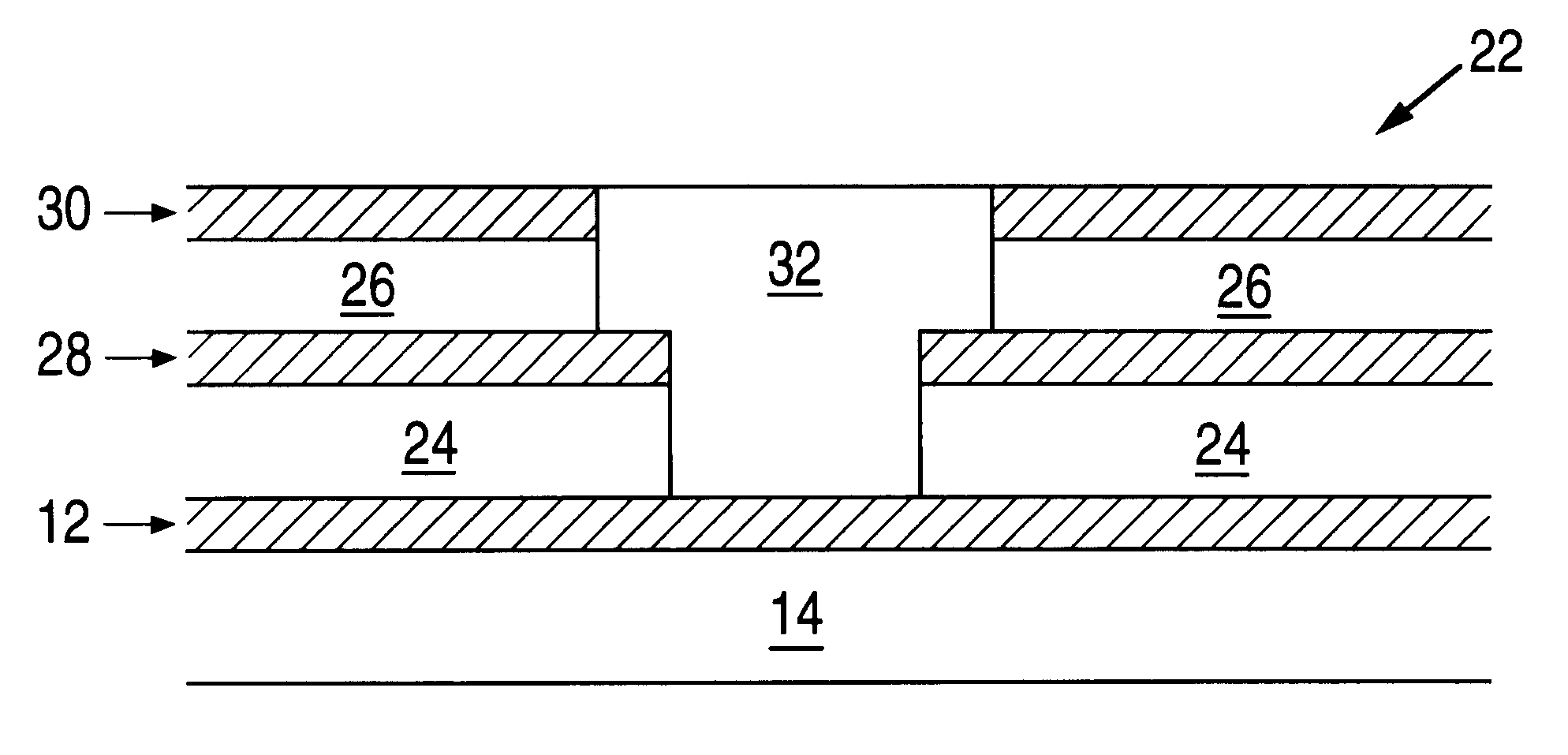
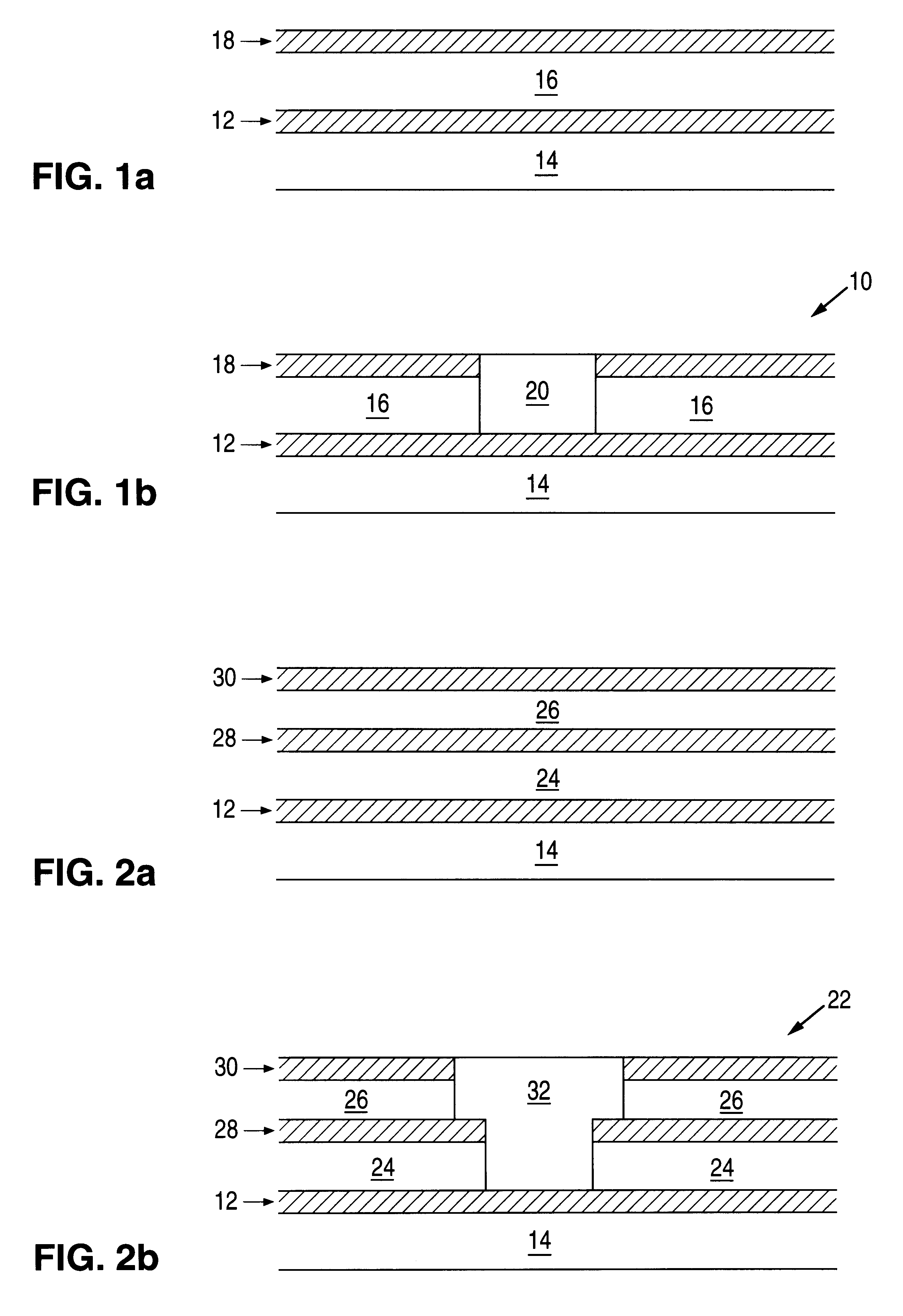
The present invention relates to methods of interconnect integration in semiconductor fabrication techniques by eliminating need for removal of the wafer after formation of a polymeric interlayer dielectric to equipment for forming conventional oxide hardmasks on interlayer dielectrics. The present invention increases device speed by reducing the effective dielectric constant in the stack, and the structures created thereby. Instead of a conventional oxide hardmask, the present invention utilizes methylated oxide-type materials as hardmasks for the interlayer dielectric. As a result, methods according to the present invention benefit from increased compatibility and improved adhesion between the hardmask and interlayer polymeric dielectric and ease of subsequent wafer processing, especially chemical mechanical polishing steps. Methylated oxide-type dielectrics contemplated for hardmasks also have similar etching characteristics to conventional oxide hardmasks so that known processin...


PUM


Abstract

Disclosed are multilevel interconnects for integrated circuit devices, especially copper/dual damascene devices, and methods of fabrication. Methylated-oxide type hardmasks are formed over polymeric interlayer dielectric materials. Preferably the hardmasks are materials having a dielectric constant of less than 3 and more preferably 2.7 or less. Advantageously, both the hardmask and the interlayer dielectric can be spincoated.

Description

1. Field of the InventionThe present invention relates to interconnect integration technology. More specifically, the present invention relates to methylated oxide-type hardmasks for patterning interlayer dielectrics in integrated circuit device fabrication.2. Description of the Related ArtIntegration of multilevel interconnects becomes increasingly important with ever increasing demands for device miniaturization and speed. In fact, with sub-0.25 .mu.m geometries, interconnect capacitance is much larger than transistor capacitance. A reduction of the interconnect capacitance decreases RC and in turn, delay, thereby in creasing device speed.Efforts to improve device performance include reducing the dielectric constant of interlayer dielectrics and the electrical resistance of interconnects, thereby reducing the wiring delay. Ikeda, et al., I.E.E.E. Inter. Interconnect Technology Conf. (1998) p. 131, describe a low k polymeric dielectric with a Cu-damtascene structure. The polymeric ...

Claims


Application Information

Patent Timeline
IPC IPC(8): H01L21/768H01L21/70H01L21/02H01L21/312H01L21/316
CPCH01L21/76807H01L21/76829H01L21/76835H01L21/3122H01L21/31612H01L21/02118H01L21/02282
Inventor ALLADA, SUDHAKARFOSTER, CHRIS
Owner NAT SEMICON CORP
Why Eureka
Try Eureka