

Magnetic thin film element, memory element using the same, and method for recording and reproducing using the memory element
a memory element and thin film technology, applied in the field of magnetic thin film elements, memory elements using the same, and methods for recording and reproducing using the memory element, can solve the problem of impossible high integration
- Summary
- Abstract
- Description
- Claims
- Application Information
AI Technical Summary
Problems solved by technology
Method used
Image

Examples
embodiment 2
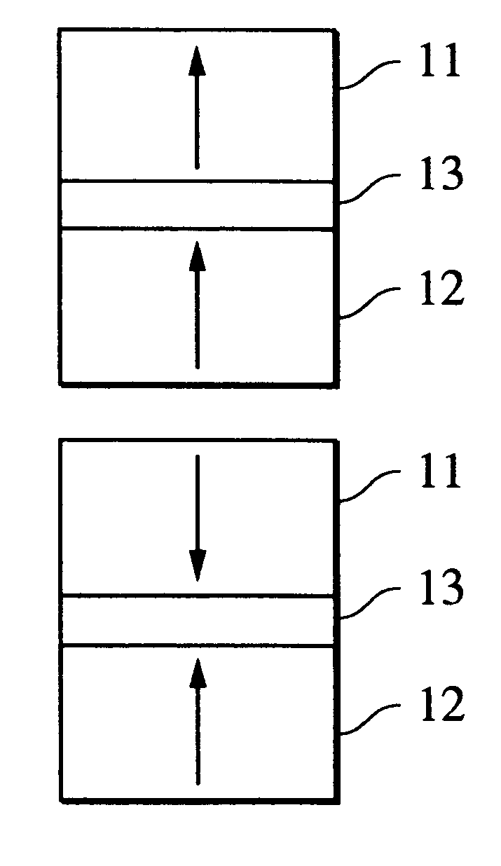
A magnetic thin film element of this embodiment has the structure shown in FIGS. 4A and 4B, and a nonmagnetic layer 13 interposed between a first magnetic layer 11 and a second magnetic layer 12 is composed of a good conductor. This element is hereinafter referred to as a spin scattering element. A good conductor preferably has higher conductivity than that of the first magnetic layer 11 or the second magnetic layer 12, and, for example, Cu may be used.
Since a good conductor having Cu as a major constituent has its Fermi energy close to that of the magnetic layer and has good adhesion, resistance easily occurs at the interface when the magnetization direction changes, and thus a large magnetoresistance ratio can be obtained. Also, preferably, the nonmagnetic layer 13 has a thickness of 5 .ANG. to 60 .ANG..
Preferably, by providing a magnetic layer having Co as a major constituent, between the first magnetic layer 11 and the nonmagnetic layer 13, or between the second magnetic layer 1...
embodiment 3
A magnetic thin film element of this embodiment has the structure shown in FIGS. 4A and 4B, and a nonmagnetic layer 13 interposed between a first magnetic layer 11 and a second magnetic layer 12 is composed of an insulator, and thus a spin-tunnel film is formed. When an electric current is applied perpendicular to the film surface during reproducing, tunneling of electrons from the first magnetic layer 11 to the second magnetic layer 12 occurs.
Since such a spin-tunnel element has a higher magnetoresistance ratio in comparison with the spin scattering element described above, output signals having a satisfactory SIN ratio can be obtained.
In the spin-tunnel magnetic thin film memory element of this embodiment, a ferromagnetic tunnel junction, which includes a ferromagnetic material, an insulator, and a ferromagnetic material, is formed. Since conduction electrons of the ferromagnetic materials tunnel while maintaining the spins, tunnel probability varies depending on the magnetization...
embodiment 4
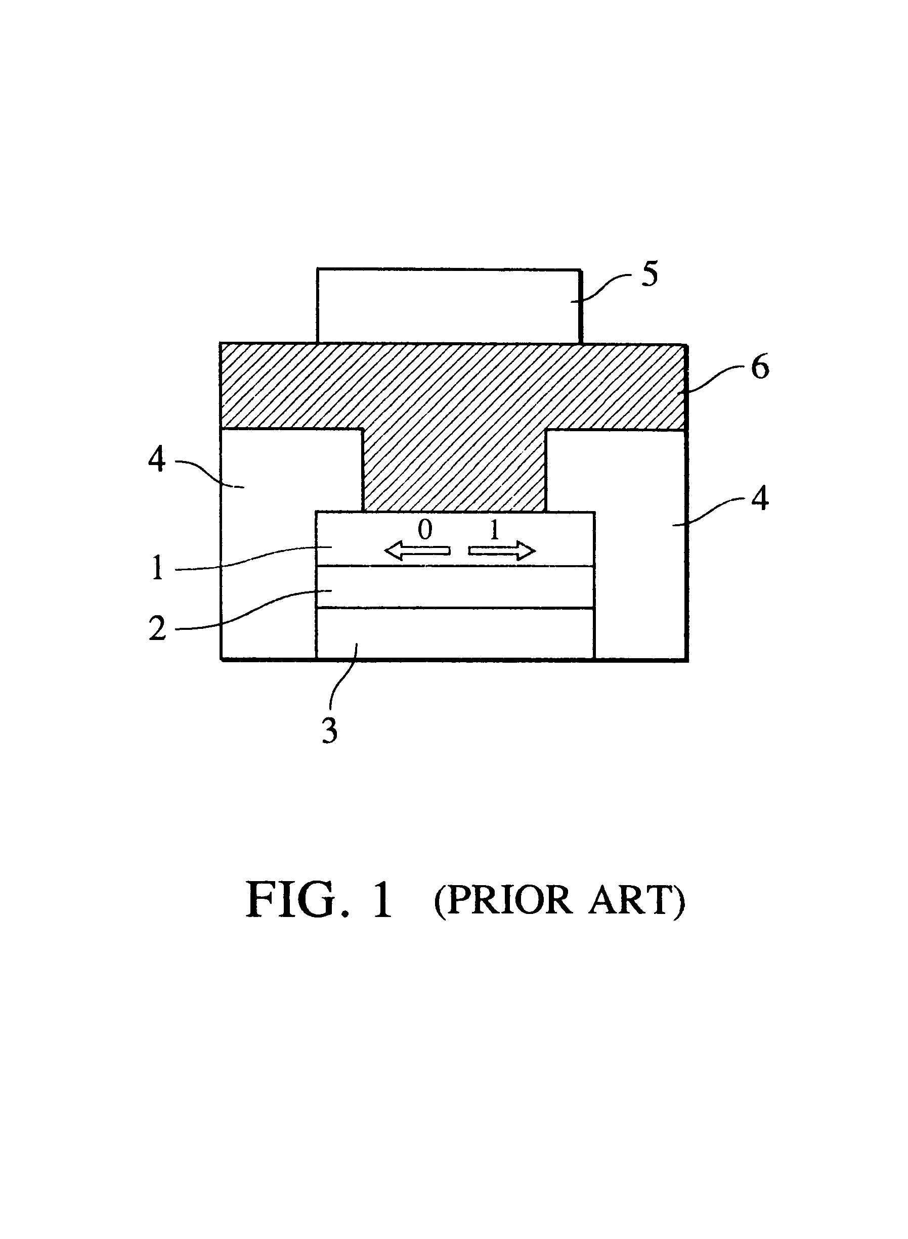
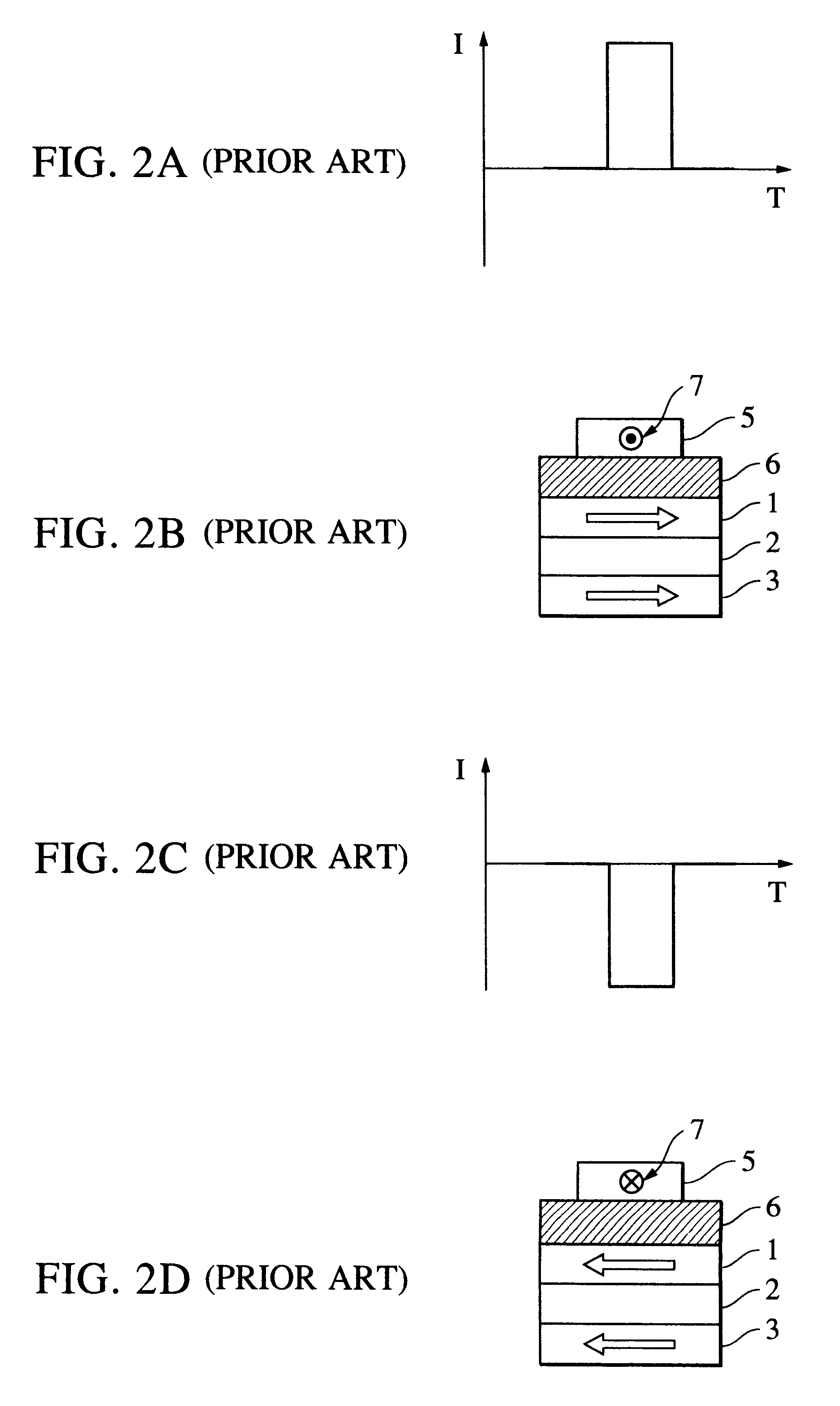
One of the applications of a magnetic thin film element in accordance with the present invention is an application to a memory element, which records information of "0" or "1" in response to the magnetization direction, and reads information using a difference in resistance.
FIG. 6 is a schematic sectional view showing a memory element which uses the magnetic thin film element described above. In FIG. 6, the same members as those in FIGS. 4A and 4B are represented by the same numerals as in FIGS. 4A and 4B, and detailed descriptions will be omitted. Numeral 14 represents the magnetic thin film element shown in FIGS. 4A and 4B, numeral 15 represents a write line composed of a good conductor, and numeral 16 represents a magnetic field generated by applying an electric current to the write line 15.
In the memory element of this embodiment, magnetization information "0" or "1" is recorded in response to the spin direction, i.e., upward or downward, of either the first magnetic layer 11 or...
PUM
 Abstract
Description
Claims
Application Information