Layered semiconductor structure for lateral current spreading, and light emitting diode including such a current spreading structure

a technology of lateral current spreading and semiconductor structure, which is applied in the direction of semiconductor devices, basic electric elements, electric devices, etc., can solve the problems of high material consumption for forming the window layer, and affecting the efficiency of the semiconductor devi

Inactive Publication Date: 2001-04-24
VISHAY SEMICON
View PDF4 Cites 15 Cited by
  • Summary
  • Abstract
  • Description
  • Claims
  • Application Information

AI Technical Summary

Problems solved by technology

It is a well known dilemma in the field of semiconductor devices, that on the one hand a current flow should be distributed as uniformly as possible over the entire active region surface of a semiconductor device such as a light emitting diode (LED), while on the other hand, the current injecting electrode or contact should be made as small as possible, i.e. covering the smallest portion of the active region surface as possible, to avoid blocking or reflecting the light emitted from the active region and for reasons of costs and complexity.
In view of the above dilemma, certain problems arise.
Therefore, it is a well known problem to provide lateral current spreading between the electrode surface and the active region surface.
A substantial disadvantage of all of the above mentioned conventional thick window layers is that the window layer has a substantially greater thickness than the active layers, which typically have thicknesses less than 1 .mu.m.
This very great thickness of the window layer leads to a high material consumption for forming the window layer, and also requires a very long time for carrying out the epitaxial growth using conventional equipment.
While it is possible to use more complicated and more expensive equipment for carrying out the epitaxial growth more quickly, it is still not possible to reduce the material consumption and costs, and the equipment costs are increased even further.
Dis

Method used


Image

  • Layered semiconductor structure for lateral current spreading, and light emitting diode including such a current spreading structure
  • Layered semiconductor structure for lateral current spreading, and light emitting diode including such a current spreading structure
  • Layered semiconductor structure for lateral current spreading, and light emitting diode including such a current spreading structure

Examples


Embodiment Construction

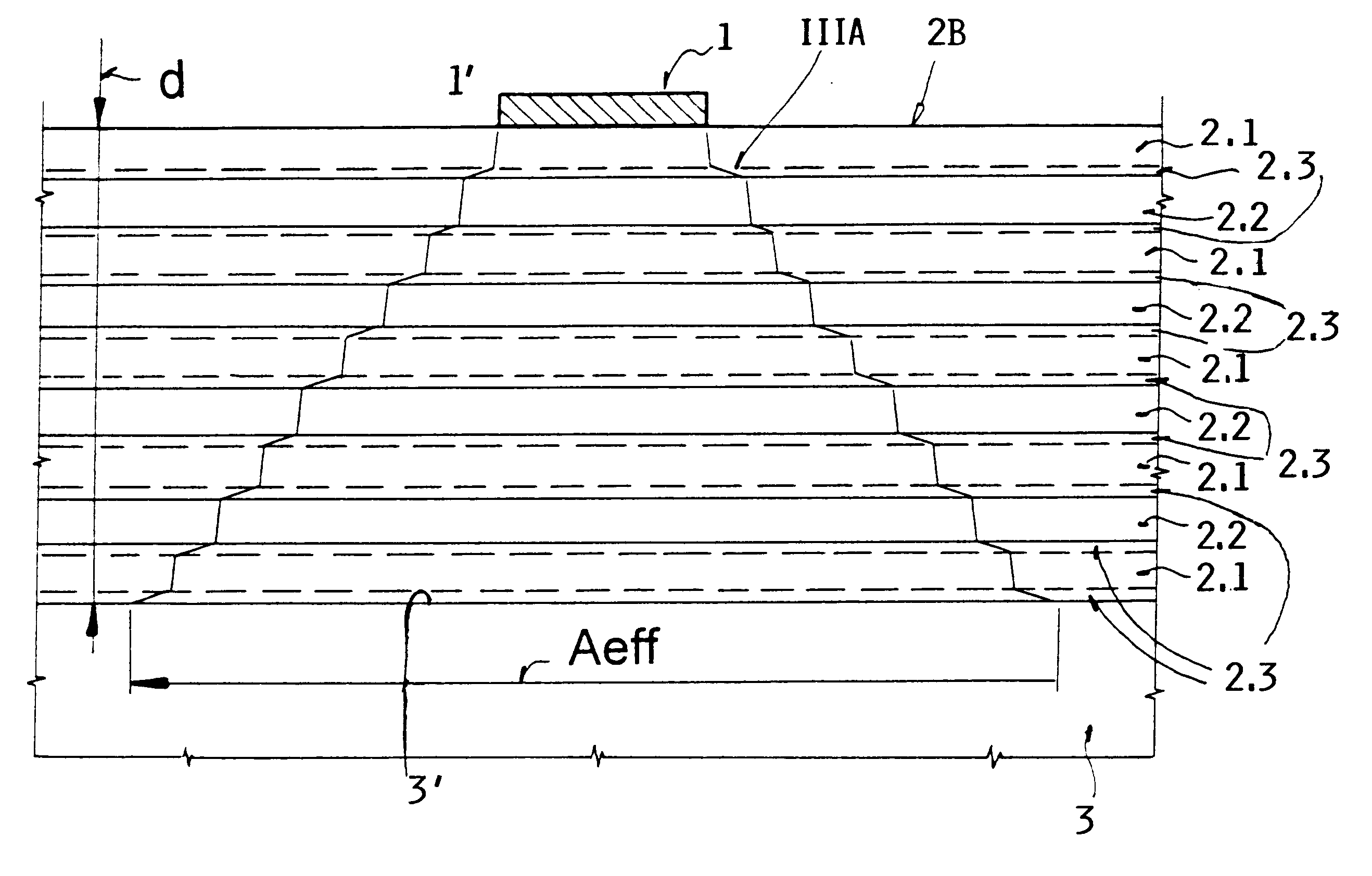
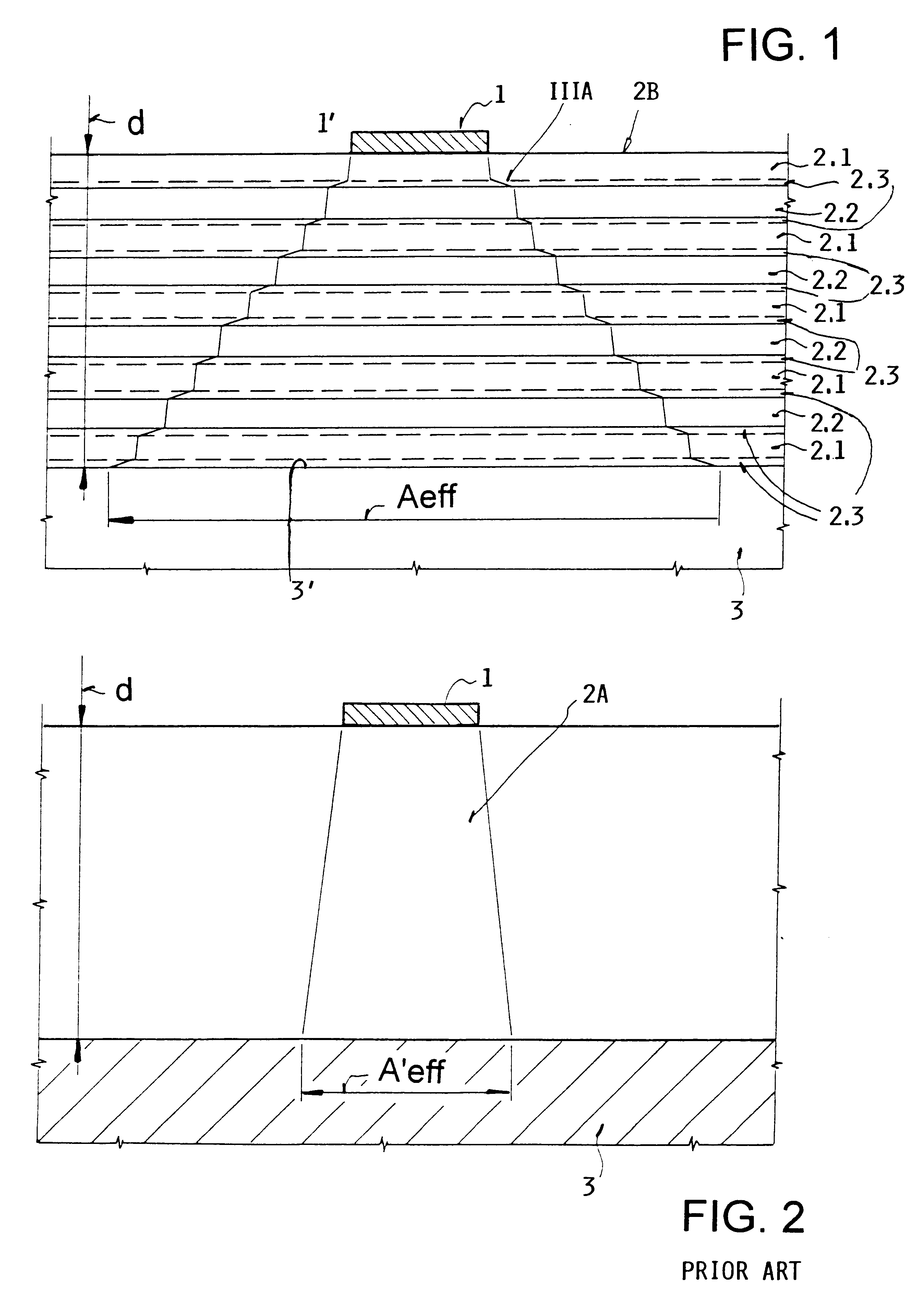
FIG. 1 shows the step-wise lateral current spreading effect in a heterostructure 2B comprising a sequence or stack of semiconductor layers forming heterojunctions 8 therebetween, arranged between the electrode surface 1' of an electrode or contact 1 and an active region surface 3' of an active region 3. The effective area of the active region surface 3' through which current flows is indicated in a simplified one-dimensional manner by the width A.sub.eff, whereby it should naturally be understood that the current spreading effect in the three-dimensional space of the heterostructure 2B actually expands outwardly in a quasi-pyramid shaped manner from the electrode surface 1' of the contact 1 to the surface 3' of the active region 3.

The heterostructure 2B comprises a sequence or stack of alternating individual semiconductor layers 2.1 and 2.2 having respective different band gaps, which is achieved by making the respective layers 2.1 and 2.2 of different semiconductor materials or dif...


PUM


Abstract

In order to achieve lateral current spreading between a current injecting or current collecting surface of an electrode and an active surface of an active region in a semiconductor device such as a light emitting diode, a layered semiconductor heterostructure is arranged between the electrode and the active surface. The heterostructure includes at least two semiconductor layers forming a heterojunction therebetween, whereby the semiconductor layers are composed of different semiconductor materials or different compositional proportions of the same compound semiconductor. An enrichment region for the majority charge carriers is formed in one of the layers adjacent the heterojunction, and a majority charge carrier energy band discontinuity exists at the heterojunction. Each enrichment region provides a strong lateral current spreading effect, such that a stacked arrangement of plural heterojunction layer pairs brings about a strong step-wise lateral current spreading. The light output and efficiency of a light emitting diode is substantially improved by incorporating such a current spreading heterostructure.

Description

PRIORITY CLAIMThis application is based on and claims the priority under 35 U.S.C. .sctn.119 of German Patent Application 197 41 609.8, filed on Sep. 20, 1997, the entire disclosure of which is incorporated herein by reference.The invention relates to a structure of semiconductor layers for conducting and laterally spreading a current between a current injection surface or current collecting surface of an electrode and an active area surface arranged parallel thereto, wherein the electrode surface has a different, e.g. smaller, surface area than the active area surface. The invention further relates to a semiconductor light emitting diode incorporating such a current spreading structure.BACKGROUND INFORMATIONIt is a well known dilemma in the field of semiconductor devices, that on the one hand a current flow should be distributed as uniformly as possible over the entire active region surface of a semiconductor device such as a light emitting diode (LED), while on the other hand, the...

Claims


Application Information

Patent Timeline
IPC IPC(8): H01L33/00H01L33/02H01L33/14H01L33/30
CPCH01L33/14H01L33/30H01L33/02
Inventor GENG, CHRISTIANGERNER, JOCHEN
Owner VISHAY SEMICON
Why Eureka
Try Eureka