Diffusion barrier enhancement for sub-micron aluminum-silicon contacts

a technology of aluminum-silicon contacts and diffusion barrier layers, which is applied in semiconductor/solid-state device manufacturing, basic electric elements, electric apparatus, etc., can solve problems such as difficulty in forming an effective barrier layer at the bottom of a contact hole with a large aspect ratio, and the effect of miniaturization

Inactive Publication Date: 2001-05-01
UNITED MICROELECTRONICS CORP
View PDF9 Cites 11 Cited by
  • Summary
  • Abstract
  • Description
  • Claims
  • Application Information

AI Technical Summary

Problems solved by technology

However, problems arise with continued miniaturization.
As the metal filled contact holes used to connect overlying interconnect wiring lines to underlying silicon regions become smaller, undesirable phenomena that are not observed in larger contact hole structures can occur.
For example, it can be difficult to form an effective barrier layer at the bottom of a contact hole which has a large aspect ratio, such as may arise for deep holes having openings of about 0.5 .mu.m across or smaller.
Such penetration, known as "spiking," can result in junction degradation, particularly when the aluminum "spike" penetrates through a source/drain region, allowing si

Method used


Image

  • Diffusion barrier enhancement for sub-micron aluminum-silicon contacts
  • Diffusion barrier enhancement for sub-micron aluminum-silicon contacts
  • Diffusion barrier enhancement for sub-micron aluminum-silicon contacts

Examples


first embodiment

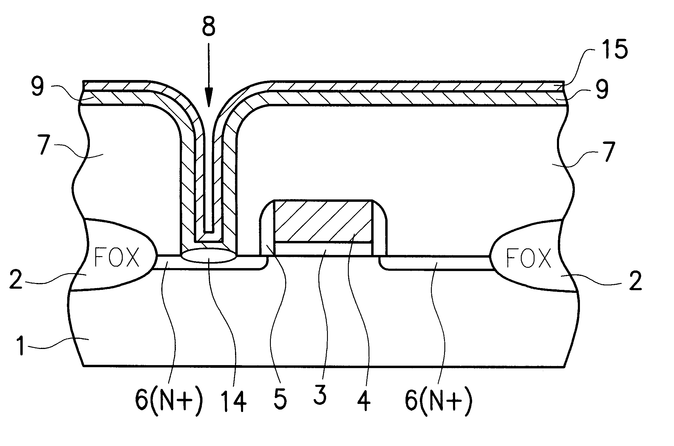
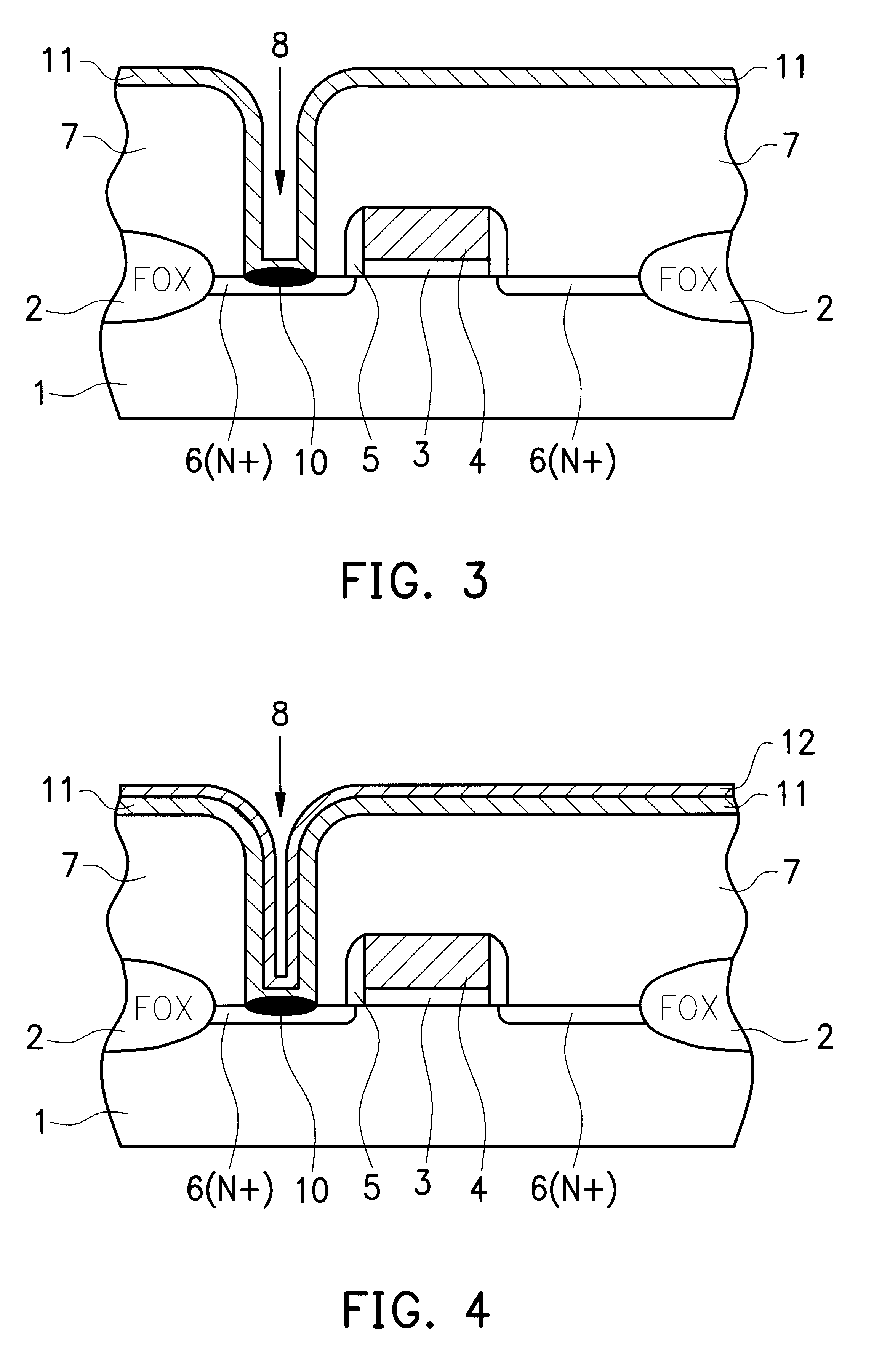
a contact structure in accordance with this invention will now be shown in FIGS. 3-4. The structure shown schematically in FIG. 2 is subjected to a rapid thermal nitridization (RTN) procedure, preferably at a temperature of between about 600 to 800.degree. C. for a preferred time between about 60 to 100 seconds, in a nitrogen, ammonia or other nitrogen-containing ambient. This procedure results in the formation of a titanium disilicide layer 10 at the bottom of contact hole 8 having a thickness of between about 200 to 500 .ANG.. The titanium disilicide layer forms an ohmic contact with the doped silicon region and thus provides a good ohmic contact between the underlying N+ region 6 and the overlying layers formed over the titanium disilicide layer in this embodiment. The RTN process, in addition to converting the bottom portion of titanium layer 9 to titanium disilicide layer 10, also converts a top or surface portion of titanium layer 9 to a titanium nitride layer 11, preferably h...


PUM


Abstract

Methods for enhancing the effectiveness of barrier layers, needed to prevent interaction between overlying aluminum interconnect metallizations, and underlying silicon device regions, has been developed. One method consists of using dual layers of titanium nitride, on titanium disilicide. The first titanium nitride layer is obtained via rapid thermal annealing of an underlying titanium layer, in a nitrogen containing ambient, also resulting in the formation of the underlying titanium disilicide layer. The second titanium nitride layer is deposited using reactive sputtering. A second method, used to create an enhanced barrier layer, is to reactively sputter titanium nitride, directly on an underlying titanium layer. Rapid thermal annealing, in an ammonia and oxygen ambient, results in an oxygen containing titanium nitride barrier layer. The rapid thermal anneal cycle also converts the underlying titanium layer, to the desired titanium disilicide layer. The barriers produced by these methods have demonstrated barrier effectiveness, in terms of preventing aluminum penetration, when compared to counterparts, fabricated without the use of the processes, described in this invention.

Description

1. Field of the InventionThis invention relates to fabrication methods used for semiconductor devices and more specifically to an improved process to create barrier films of the type used to separate aluminum-based metallizations from silicon regions contacted thereby.2. Description of the Related ArtThe semiconductor industry continually strives to increase device performance while maintaining or decreasing the cost of manufacturing advanced silicon chips. These objectives have been realized, in part, by the ability of the semiconductor industry to achieve silicon device miniaturization. The ability to produce silicon devices with sub-micron critical features has resulted in significant device performance improvements, for example by reducing the resistance of metal interconnect wiring, as well as reducing capacitance with underlying silicon device regions. Miniaturization has also contributed to cost reductions. The ability to reduce critical device dimensions has led to a signifi...

Claims


Application Information

Patent Timeline
IPC IPC(8): H01L21/768H01L21/70
CPCH01L21/76843H01L21/76855H01L21/76856
Inventor YANG, CHI-CHENGKUO, KUO-YUNLIN, JENN-TARNG
Owner UNITED MICROELECTRONICS CORP
Why Eureka
Try Eureka