Dielectrically isolated IC driver having upper-side and lower-side arm drivers and power IC having the same

a technology of dielectric isolation and ic driver, which is applied in the direction of pulse technique, electronic switching, semiconductor devices, etc., can solve the problems of unstable operation of the upper-side driver 102, power supply voltage drop, and low output voltag

Inactive Publication Date: 2001-05-01
KK TOSHIBA
View PDF1 Cites 43 Cited by
  • Summary
  • Abstract
  • Description
  • Claims
  • Application Information

AI Technical Summary

Problems solved by technology

Additionally, if the displacement current J.sub.d flows over the driving capability of the internal power supply circuit 105, the power supply voltage decreases, making the operation of the upper-side driver 102 unstable.
Or, even then the driving capability is not exceeded, a sudden load variation will cause a time lag to feedback this situation, provoking a lower output voltage with this time lag.
Moreover, a larger internal power supply circuit 105 increases the power dissipation of the driving circuit, lowering the total power conversion efficiency of the system.
Even in an nMOS transistor, npn bipolar transistor, pnp bipolar transistor, or other semiconductor devices such as diode, such problem may happen in a DI integrated circuit of the structure having a p diffusion layer or n diffusion layer forming the semiconductor island presenting the floating state and where this p diffusion layer or n diffusion layer is connected to the internal power supply circuit or other circuit than the internal power supply circuit.
For example, a similar problem may happen in a case where a p well exists in an n type semiconductor island and an nMOS transistor is formed therein.
However, in the nMOS transistor where the p well is used in floating state, namely lifted from the reference potential, the displacement current J.sub.d flows in the bottom parasitic MOS (MIS) structure, and the extra current of the internal power supply circuit increases excessively, to lower the output voltage of the internal power supply circuit disadvantageously or to affect the other circuit than the internal power supply circuit to fluctuate the circuit parameters and circuit operation detrimentally.
Then electrons can be injected from the n diffused layer, causing similar disadvantage as the case for the p diffused layer.
Therefore, the displacement current J.sub.d in the bottom of parasitic MOS (MIS) structure becomes significant in various situations and various structures irrespective of p or n diffused layer, to make circuit parameters of the DI integrated circuit seriously changeable and unreliable.

Method used


Image

  • Dielectrically isolated IC driver having upper-side and lower-side arm drivers and power IC having the same
  • Dielectrically isolated IC driver having upper-side and lower-side arm drivers and power IC having the same
  • Dielectrically isolated IC driver having upper-side and lower-side arm drivers and power IC having the same

Examples


first embodiment

FIG. 7A is a circuit diagram showing a portion extracted from the upper-side driver of the IC driver according to the present invention shown in FIG. 6. CMOS inverter 111 is composed of a pMOS transistor Q.sub.pp and nMOS transistor Q.sub.nn. A source electrode (first main electrode) of the pMOS transistor Q.sub.pp is connected to the internal power supply circuit 105 and a drain electrode (second main electrode) to the drain electrode of the nMOS transistor Q.sub.nn. And a substrate electrode of the pMOS transistor Q.sub.pp is connected simultaneously to the source electrode of the pMOS transistor Q.sub.pp, and to the intermediate potential terminal N.sub.n2 through a bypass diode D.sub.bp.

FIG. 7B is a partial plan view corresponding to FIG. 7A, and shows plurality of semiconductor islands 147, 148, 149, 157, 158, 159, . . . Namely FIG. 7B shows in details a partial plan view of the CMOS inverter 111. Meanwhile, the lower-side driver 103 having the CMOS inverter 112 disposed in a s...

second embodiment

(SECOND EMBODIMENT)

FIGS. 17A to 17C are partial cross-sectional views illustrating the variation of the depletion layer width in accordance with the variation of the potential (intermediate potential) at the intermediate potential terminal N.sub.n2 of the IC driver according to a second embodiment of the present invention. As shown in FIGS. 17A to 17C, the IC driver according to the second embodiment of the present invention comprises at least semiconductor island (n.sup.- type semiconductor island) 147 separated by the bottom dielectric film 12 and the side dielectric film 6, a switching device in a floating state (pMOS transistor) disposed in this n.sup.- type semiconductor island 147, and an injector region 245 disposed in the n.sup.- type semiconductor island 147, at a position separated from the switching device, for injecting carriers having conduction type identical to that of the carrier constituting the main current of the switching device. Namely, FIGS. 17A to 17C are cros...

third embodiment

(THIRD EMBODIMENT)

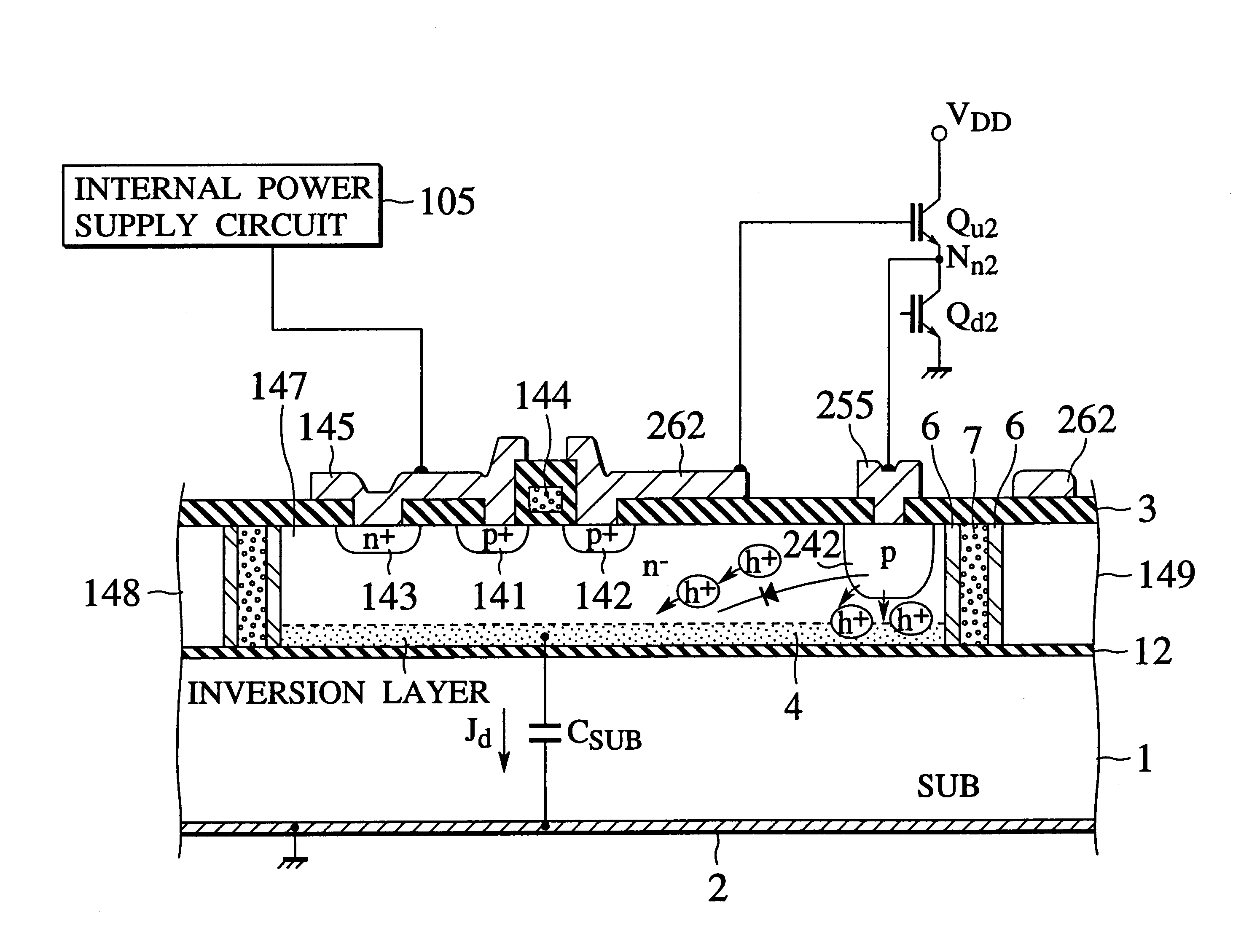
FIG. 18A is a equivalent circuit diagram to explain the drawback of the conventional IC driver comparing with the IC driver according to a third embodiment of the present invention. Namely, FIG. 18A illustrates a part of the upper-side driver 102 shown in FIG. 3, or the CMOS inverter 111 in the upper-side driver 102 and the parasitic condenser of this inverter 111. As shown in FIG. 18A, the CMOS inverter 111 is composed of pMOS transistor Q.sub.p1 and the nMOS transistor Q.sub.n1, and its output is input into the gate electrode of the IGBT serving as the upper-side output power device Q.sub.u2. FIG. 18B illustrates schematically the cross-sectional view of the pMOS transistor Q.sub.u1 in this CMOS inverter 111.

As shown in FIG. 18B, a floating state pMOS transistor Q.sub.p1 is disposed in an semiconductor island (n.sup.- type semiconductor island) 147, whose bottom is separated by an SOI oxide film (buried insulation film) 12 disposed on the n type supporting substr...


PUM


Abstract

In an IC driver using SOI dielectric isolation structure having a lower and an upper arm side drivers, the upper arm side driver operates in a floating state, a carrier injector region is disposed in an semiconductor island where a switching device for the upper-side circuit is formed. The IC driver drives a set of an upper-side and a lower-side output power devices, a first main electrode of the upper-side output power device is connected to a high level power supply, a second main electrode of the upper-side output power device is connected to a first main electrode of the lower-side output power device, a second main electrode of the lower-side output power device is connected to ground potential (GND). The carrier injector region is formed deeper than a couple of main electrode regions of the switching device in the upper arm side driver. Moreover, this injector region is connected to an intermediate potential at connecting terminal of the upper-side and the lower-side output power devices. A current for compensating the displacement current Jd flowing in the parasitic condenser CSUB inherent to the SOI structure is supplied through the carrier injector from this intermediate potential terminal, to diminish the extra load of the internal power supply circuit for supplying the upper arm side driver with a predetermined voltage.

Description

1. Field of the InventionThe present invention relates to an integrated circuit having dielectric isolation regions, which switches at a high speed, and more particularly, an IC driver capable of driving output power devices operating with a high breakdown voltage or a high blocking voltage at the high speed. The present invention also relates to a power integrated circuit (referred to as "power IC" hereinafter) merging output power devices and driver / controller for driving / controlling the output power devices in a same semiconductor chip, the chip having dielectric isolation regions, the power IC operating with a high breakdown voltage or a high blocking voltage at the high speed.2. Description of the Related ArtA semiconductor integrated circuit--using SOI structure where a supporting substrate 1, a buried insulation film (SOI oxide film) 12, and Si films 140, 147, 139, 138, 137 are stacked beginning from the bottom as shown in FIG. 1--is characterized by an easiness for accomplis...

Claims


Application Information

Patent Timeline
Patent Type & Authority Patents(United States)
IPC IPC(8): H01L27/12H01L21/762H01L21/70H03K17/06H01L21/76H01L27/08H01L29/786
CPCH01L21/76264H01L27/1203H03K17/063H01L21/76286
Inventor ENDO, KOICHIARAI, HARUKIMASUDA, KUMIKOSATO, NOBUYUKI
Owner KK TOSHIBA
Why Eureka
Try Eureka