Magnetic thin film memory, method of writing information in it, and me

a thin film memory and magnetic field technology, applied in the field of magnetic thin film memory, can solve the problems that the magnetic field necessary for writing cannot be effectively applied to the magnetoresistive thin film, and it is difficult to improve the degree of integration

Inactive Publication Date: 2001-05-01
CANON KK
View PDF3 Cites 228 Cited by
  • Summary
  • Abstract
  • Description
  • Claims
  • Application Information

AI Technical Summary

Problems solved by technology

As mentioned above, an conventional magnetic thin film memory uses a wire functioning as a bit wire and as a writing wire, and the current passed through the bit wire when writing the information may also flow into the magnetoresistive thin film itself since the magnetoresistive thin film is made of a metal material, whereby the magnetic field necessary for the writing cannot effectively be applied to the magnetoresistive thin film.
Thus, a conventional magnetic thin film memory has a complex structure since the number of lines of wires is large, and it is difficult to improve the degree of integration, since the area of a memory cell is wide.

Method used


Image

  • Magnetic thin film memory, method of writing information in it, and me
  • Magnetic thin film memory, method of writing information in it, and me
  • Magnetic thin film memory, method of writing information in it, and me

Examples


first embodiment

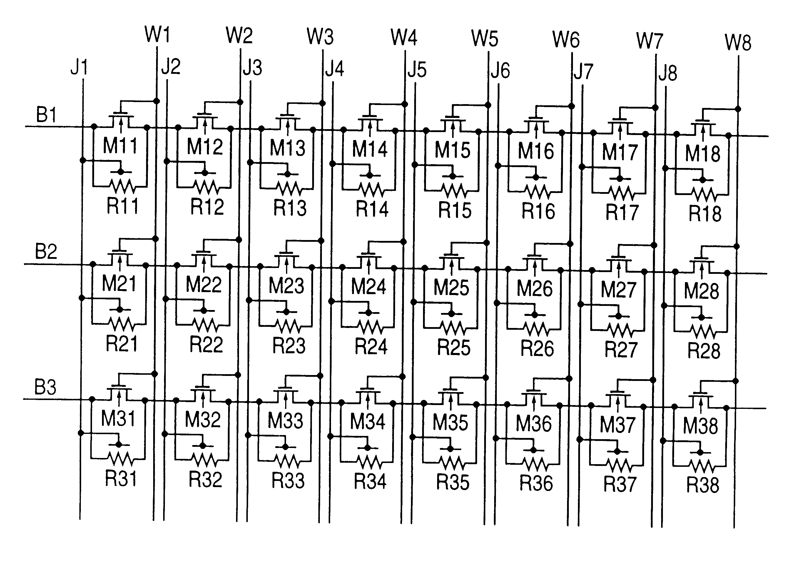
FIG. 7 is a circuit diagram showing the configuration of a magnetic thin film memory of the present invention. The reference characters R1 to R4 denote magnetoresistive thin films utilizing the giant magneto-resistance effect, and each of M11 to M14 denotes a metal / oxide / semiconductor field effect transistor (hereafter, referred to as "MOSFET"), and B1 denotes a bit wire, and J1 to J4 denote writing wires, and W1 to W4 denote word wires. A magnetic thin film memory of the present invention has a configuration in which a plurality of magnetic semiconductor hybrid elements each having a magnetoresistive thin film and a MOSFET connected in parallel are connected in series. By the way, FIG. 7 shows an example of connecting in series four magnetic semiconductor hybrid elements, but it is possible to operate as a magnetic thin film memory when two or more magnetic semiconductor hybrid elements are connected.

Each of FIG. 8A and FIG. 8B shows the structure of one selected from the magnetore...

second embodiment

In the present embodiment, an example of the device structure of a magnetic thin film memory in a case of using a method in which the direction of the current when reading the information is perpendicular to the magnetoresistive thin film 10 (hereafter, referred to as "CPP method") will be described by referring to FIG. 10. As shown in FIG. 10, the magnetoresistive thin film 10 is connected to the n-type region 21 through a lower electrode 72 and a connecting electrode 61. Further, an upper electrode 71 is arranged on the magnetoresistive thin film 10. The upper electrode 71 and the lower electrode 72 are commonly used for one magnetoresistive thin film and another adjacent magnetoresistive thin film 10. Furthermore, above the upper electrode 71 of the magnetoresistive thin film 10, the writing wire 14 is arranged. In case of using the device structure shown in FIG. 10, it is also possible that the magnetic layer 11 constituting the magnetoresistive thin film 10 is replaced by the u...

third embodiment

In the present embodiment, there will be described an example of the circuit and the device structure of a magnetic thin film memory in which the writing wire 14 in the device structure shown in FIG. 9 is replaced by the gate electrode 20 including a word wire.

FIG. 11 shows a circuit diagram in the case where the gate electrodes of the MOSFET M11 to MOSFET M14 shown in FIG. 7 are substituted for the writing wires W1 to W4. The gate wires of the MOSFET M11 to MOSFET M 14 are provided near the magnetoresistive thin films R1 to R4, which is not shown in FIG. 11.

FIG. 12 shows an example of the device structure of the circuit of FIG. 11. It is the same as the device structure shown in FIG. 9 except that the writing wire 14 is not arranged above the magnetoresistive thin film 10. In the gate electrode 20, a current as a writing current flows from the front side of FIG. 12 to the back side or from the back side of FIG. 12 to the front side. Depending on the direction of this current, magne...


PUM


Abstract

The present invention relates to a magnetic thin film memory having a hybrid element including a field effect transistor and a magnetoresistive thin film connected to the field effect transistor in parallel. In the magnetic thin film memory, the hybrid element is preferably arranged in plurality in a matrix state. The present invention also relates to a method of writing information in this magnetic thin film memory, and a method of reading the information written in this magnetic thin film memory.

Description

1. Field of the InventionThe present invention relates to a magnetic thin film memory, a method of writing information in this magnetic thin film memory, and a method of reading the information written in this magnetic thin film memory.2. Related Background ArtRecently, the development of devices including a thin film magnetic head to which the magneto-resistance effect is applied has been promoted. Among them, a magnetic thin film memory using a magnetoresistive thin film is noted, which can be substituted for a DRAM or an EEPROM used at present. Since the magnitude of resistance of a magnetoresistive thin film can largely be changed by the state of magnetization of the magnetism, a nonvolatile solid memory can be realized by combining the magnetoresistive thin film with a semiconductor device such as a transistor.As a conventional magnetic thin film memory, for example, a memory is proposed in Japanese Patent Application Laid-Open No. 6-84347, which is formed by connecting a magne...

Claims


Application Information

Patent Timeline
Patent Type & Authority Patents(United States)
IPC IPC(8): G11C11/02G11C11/15H01L21/8246H01L27/105H01L27/22H01L43/08
CPCB82Y10/00G11C11/15H01L27/228H10B61/22
Inventor NISHIMURA, NAOKI
Owner CANON KK
Why Eureka
Try Eureka