Method of measuring oxide thickness during semiconductor fabrication

a technology of semiconductor wafers and thin insulating layers, which is applied in the direction of individual semiconductor device testing, semiconductor/solid-state device testing/measurement, instruments, etc., can solve the problems of oxide build-up on solder joints, difficult to minimize or eliminate, and compromise the chip's mechanical integrity

Inactive Publication Date: 2001-05-08
IBM CORP
View PDF16 Cites 15 Cited by
  • Summary
  • Abstract
  • Description
  • Claims
  • Application Information

AI Technical Summary

Benefits of technology

It is yet another object of the present invention to provide a real-time, non-destructive measurement of oxide layer thickness on a C4 solder connection of a semiconductor substrate.

Problems solved by technology

A thin layer of metal oxide on the surface of these solder joints will detrimentally contribute to failed electrical connections, and may compromise the chip's mechanical integrity.
The metal oxides are non-conductive, having depositions that are difficult to minimize or eliminate.
Oxide build-up on solder joints, such as the C4 balls, poses unique problems to the integrated circuit chip manufacturer.
Oxide thickness has been monitored previously within the art; however, the measurement techniques implemented have been limited in speed and simplicity, and at times have been shown to be destructive to the device under test.
This, however, is considered a destructive test since the punch-through voltage is capable of delivering additional electrical stress to the product.
Additionally, these methods are not well suited for in-situ monitoring during wafer fabrication.
The equipment necessary for implementation is costly and burdensome to operate, typically requiring specially trained technicians.

Method used


Image

  • Method of measuring oxide thickness during semiconductor fabrication
  • Method of measuring oxide thickness during semiconductor fabrication
  • Method of measuring oxide thickness during semiconductor fabrication

Examples


Embodiment Construction

)

In describing the preferred embodiment of the present invention, reference will be made herein to FIGS. 1-5 of the drawings in which like numerals refer to like features of the invention. Features of the invention are not necessarily shown to scale in the drawings.

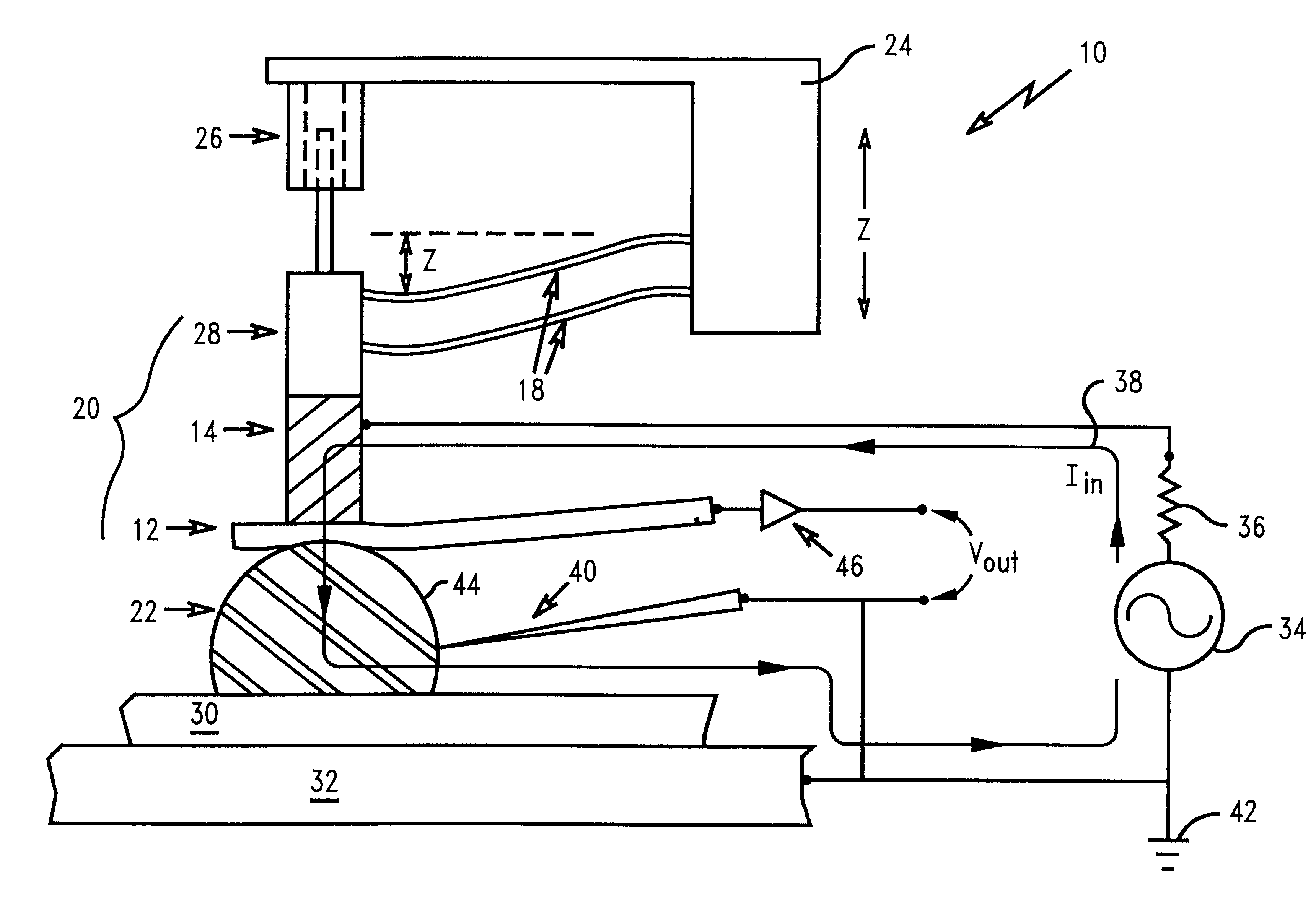
Simplicity and test speed provide unique advantages over the existing prior art for measuring oxide layer thickness in-situ during wafer fabrication. A method of utilizing the measurement of common electrical parameters, and correlating these measurements to known deviations in oxide thickness, provides a low-cost, expeditious approach for monitoring oxide films.

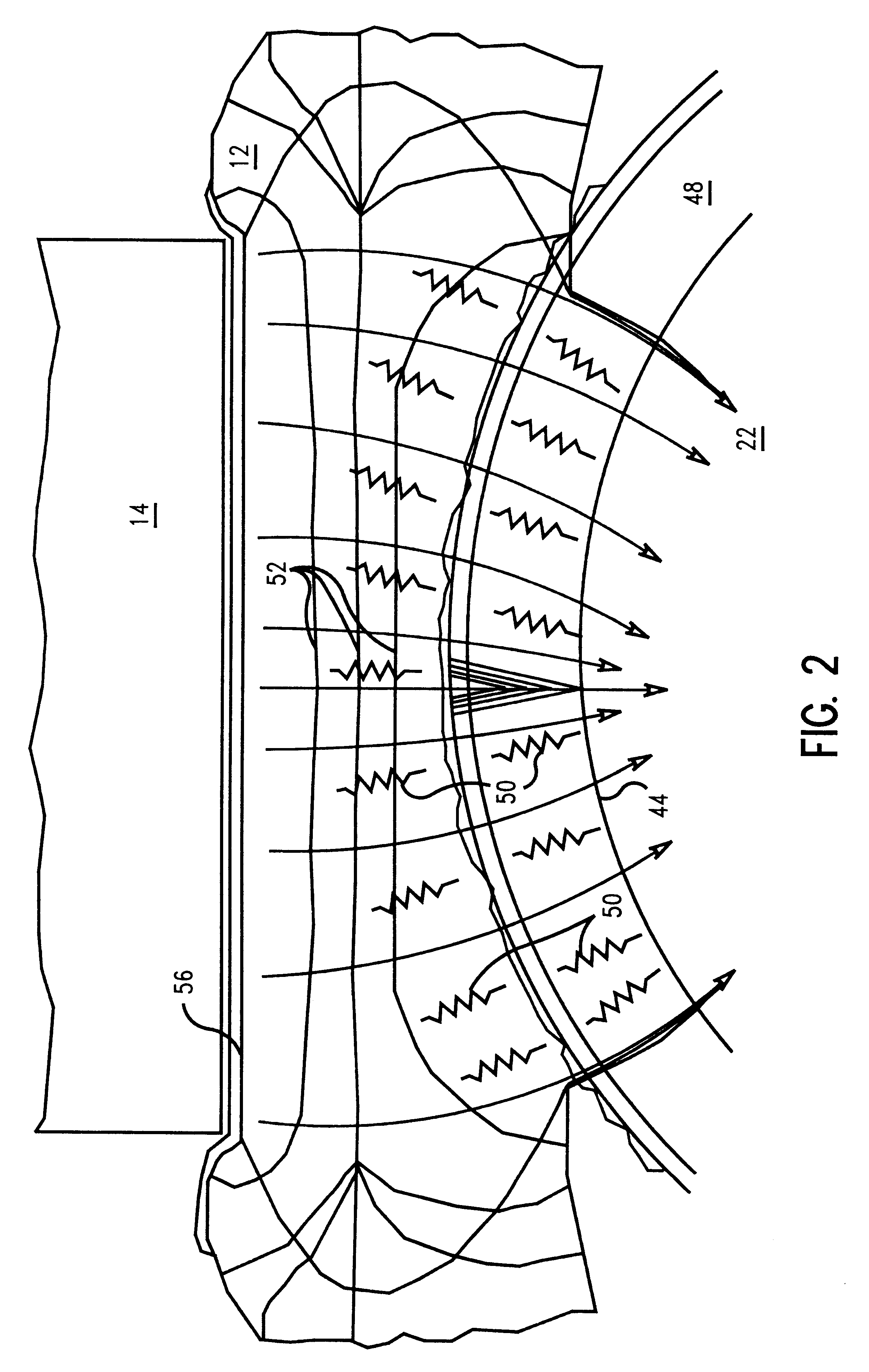
Residual oxide films build-up on solder joints during fabrication with the detrimental effect of prohibiting wetting or solderability, and insulating the electrically conductive solder joint. It is necessary for manufacturers to measure this oxide build-up accurately, and in real-time, during semiconductor wafer processing. Measuring both the capacitive and reacti...


PUM


Abstract

A measurement of thickness of a metal oxide layer on a solder ball connection during semiconductor fabrication is demonstrated by an in-situ capacitance measurement of the oxide layer. A linear relationship is shown between the reactance of the metal oxide and its thickness. This linearity is derived empirically, and correlated to Auger Spectroscopy test results for accuracy. The linear relationship demonstrated with these measurements exhibits a linear correlation coefficient, R2, greater than or equal to 0.974. This close, linear relationship allows for accurate testing of the oxide thickness using standard electrical parameter measurements during wafer fabrication.The method requires the determination of an analytical relationship between dielectric thickness and dielectric capacitance; the performance of an in-situ test of the dielectric layer capacitance including measuring the dielectric layer capacitance; and, the calculation of the dielectric layer thickness by using reactance values, calculated from the measured dielectric layer capacitance, as a variable within the analytical relationship.

Description

1. Field of the InventionThe present invention relates generally to techniques for measuring thin insulating layers on a semiconductor wafer, and more particularly, to measurements of very thin metal oxide layers accumulated on C4 solder connections.2. Description of Related ArtSolder connections composed of PbSn material are generally used for electrical and mechanical attachment for integrated circuit fabrication. Undesired residual metal oxides on the surface of C4 solder connections or balls can prevent an integrated circuit chip from successfully joining or wetting to a chip carrier. A thin layer of metal oxide on the surface of these solder joints will detrimentally contribute to failed electrical connections, and may compromise the chip's mechanical integrity. The metal oxides are non-conductive, having depositions that are difficult to minimize or eliminate. Oxide build-up on solder joints, such as the C4 balls, poses unique problems to the integrated circuit chip manufactur...

Claims


Application Information

Patent Timeline
Patent Type & Authority Patents(United States)
IPC IPC(8): H01L21/66
CPCH01L22/12
Inventor GRIFFITH, JONATHAN H.SMITH, RONALD L.VERKUIL, ROGER L.
Owner IBM CORP
Why Eureka
Try Eureka