Bistable nematic liquid crystal device

a liquid crystal device and nematic technology, applied in liquid crystal compositions, instruments, chemistry apparatuses and processes, etc., can solve the problems of low shock resistance, small portable size, and high voltage needed to switch materials,

Inactive Publication Date: 2001-06-19
ZBD DISPLAY LTD
View PDF5 Cites 106 Cited by
  • Summary
  • Abstract
  • Description
  • Claims
  • Application Information

AI Technical Summary

Problems solved by technology

One disadvantage of ferroelectric devices is the relatively large voltage needed to switch the material.
This high voltage makes small portable, battery powered displays expensive.
Also these displays suffer from other problems such as lack of, shock resistance, limited temperature range and also electrically induced defects such as needles.
However this method suffers the disadvantage that any deviation in the evaporation angle, ...

Method used


Image

  • Bistable nematic liquid crystal device
  • Bistable nematic liquid crystal device
  • Bistable nematic liquid crystal device

Examples


example 1

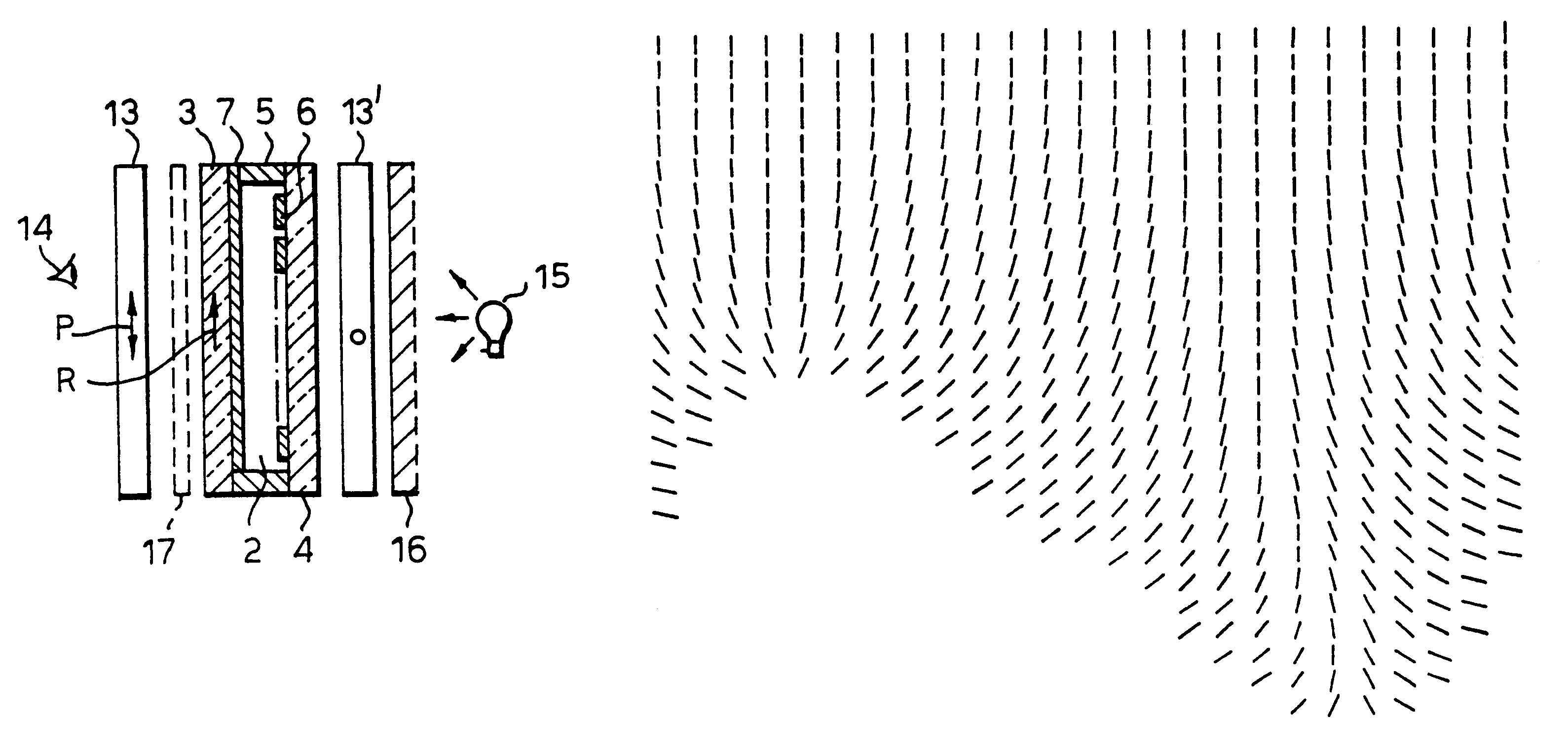
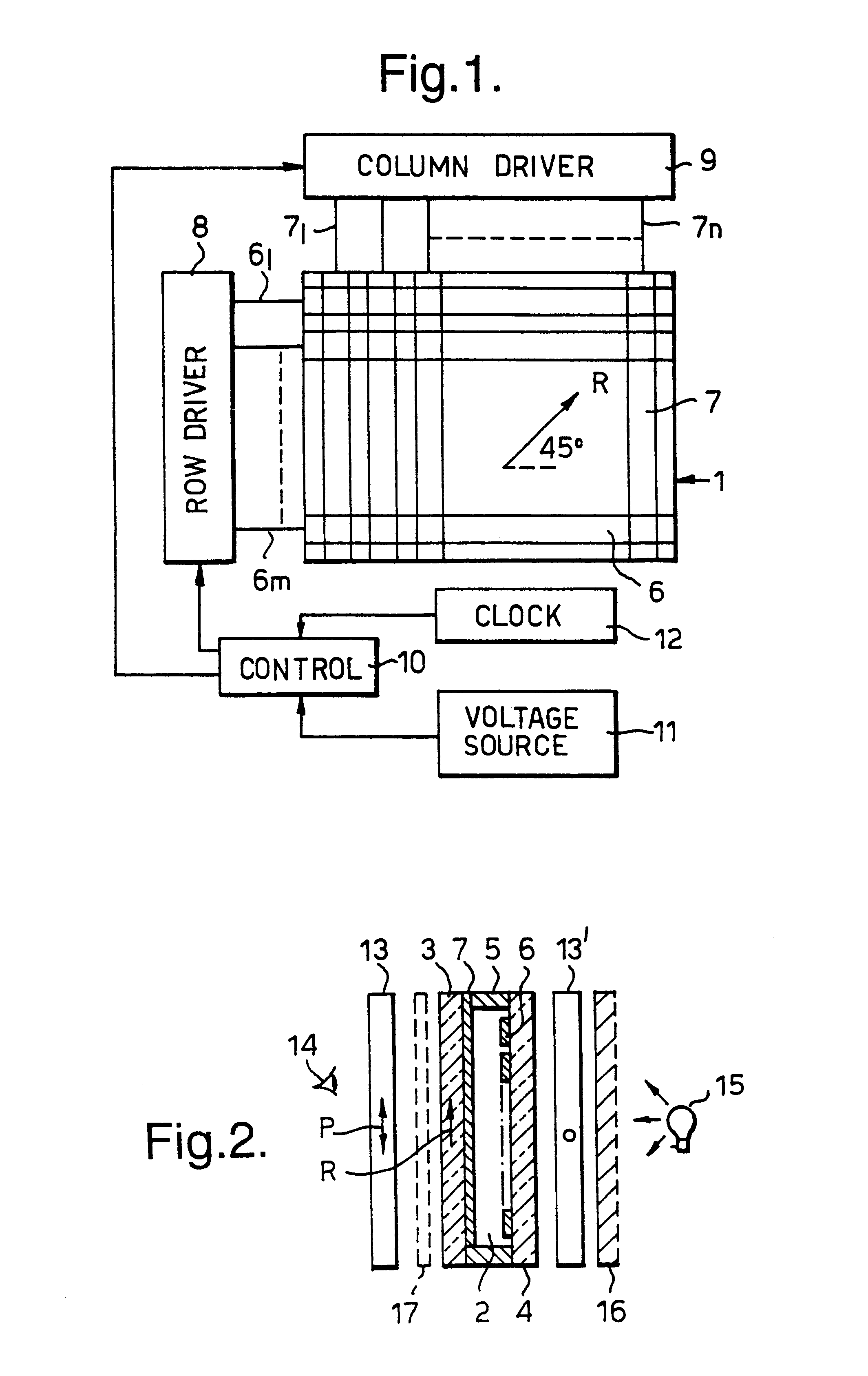
A piece of ITO coated glass to form the cell wall 3, 4 was cleaned with acetone and isopropanol and was then spin coated with photoresist (Shipley 1805) at 3000 rpm for 30 seconds giving a coating thickness of 0.55 .mu.m. Softbaking was then carried out at 90.degree. C. for 30 minutes.

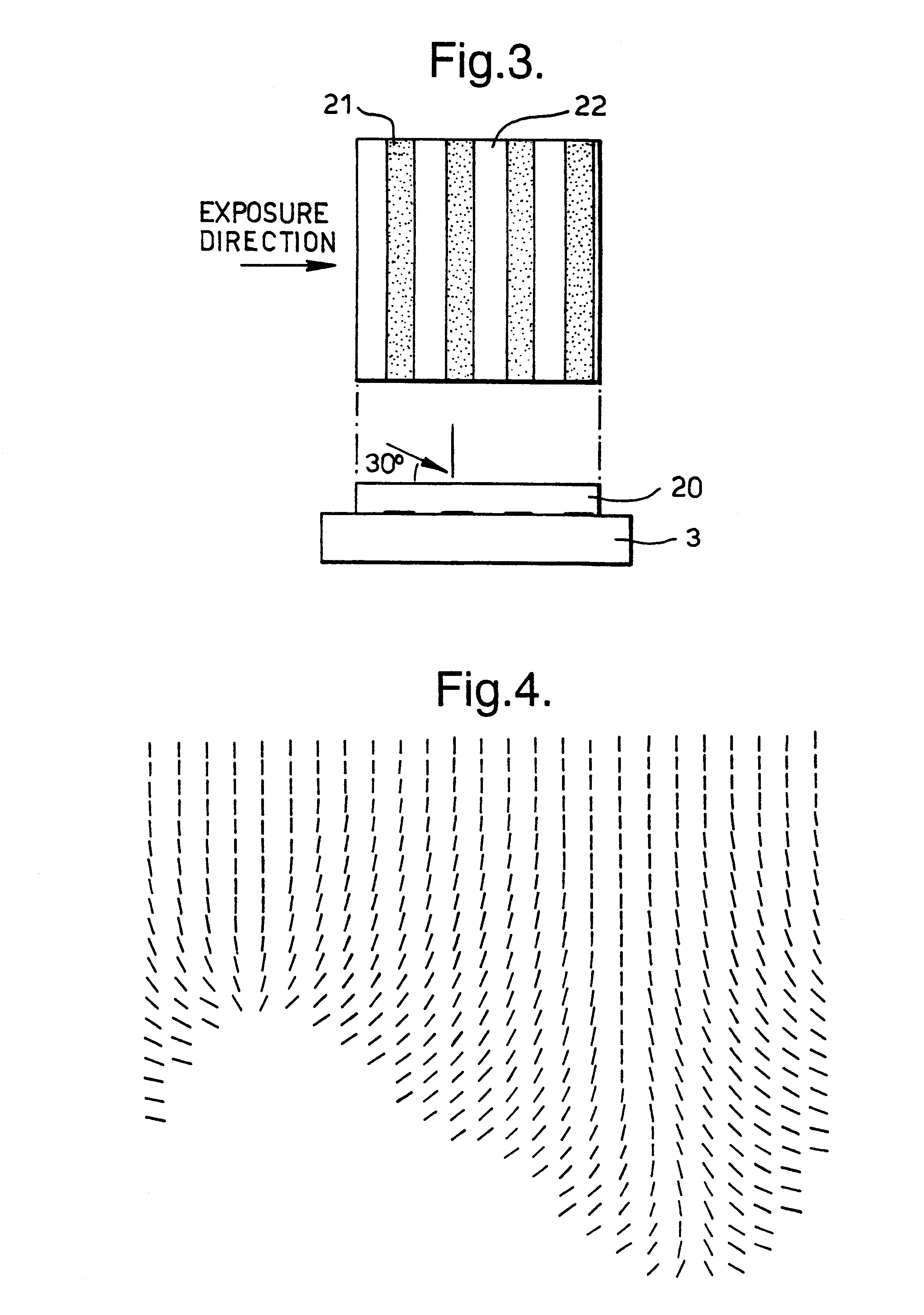
A contact exposure was then carried out on the coated wall 3, 4 using a chrome mask 20 containing 0.5 .mu.m lines 21 and 0.5 .mu.m gaps 22 (hence an overall pitch of 1 .mu.m) as shown in FIG. 3. The exposure was carried out at non-normal incidence, in this case an angle of 60.degree. was used. Mask 20 orientation is such that the groove direction is substantially perpendicular to the to plane of incidence as shown in FIG. 3. Exposure in this geometry leads to an asymmetric intensity distribution and therefore an asymmetric grating profile (see for example B. J. Lin, J. Opt. Soc. Am., 62, 976 (1972) ). Coated cell walls 3, 4 were exposed to light from a mercury lamp (Osram Hg / 100) with an intensity of 0...

example 2

A second example of a bistable device is now described. A piece of ITO coated glass to form the cell wall was cleaned with acetone and isopropanol and was then spin coated with photoresist (Shipley 1813) at 3000 rpm for 30 seconds giving a coating thickness of 1.5 .mu.m. Softbaking was then carried out at 90.degree. C. for 30 minutes.

A contact exposure was then carried out using a chrome mask containing 0.5 .mu.m lines and 0.5 .mu.m gaps (hence an overall pitch of 1 .mu.m). In this example the exposure was carried out at normal incidence. Exposure in this geometry leads to a symmetric intensity distribution and therefore a symmetric grating profile. Samples were exposed to light from a mercury lamp (Osram Hg / 100) with an intensity of 0.8 mW / cm.sup.2.

After the exposure the sample was released from the mask and developed in Shipley MF319 for 20 seconds followed by a rinse in de-ionised water. This left the sample patterned with a symmetric surface modulation. The photoresist was then ...

example 3

The bistable grating surface can also be constructed opposite a planar surface. One such cell consisted of a grating with the same profile to that described in example 2. This was constructed opposite a rubbed polymer surface formed using a layer of PI32 polyimide (Ciba Geigy). The rubbing direction on the polyimide surface was set parallel to the grating groove direction on the grating surface. The cell gap was set to 2.5 .mu.m and nematic E7 was used to fill the cell. Cooling to room temperature after filling revealed two states which are shown schematically in FIGS. 11(a) and 11(b). This Figure differs from FIGS. 7(a) and 7(b) in that the groove direction on the bistable surface is now in the plane of the page (in an x,y plane). Thus the 90.degree. pretilt state on the grating forms the hybrid structure shown in (a') while the 0.degree. pretilt state on the grating forms the twisted structure shown in (b'). To achieve optical contrast between the states, the cell was placed in-be...


PUM


Abstract

A bistable nematic liquid crystal device cell (1) is provided with a surface alignment grating on at least one cell wall (3) and a surface treatment on the other wall (4). Such treatment may be a homeotropic alignment or a planar alignment with or without an alignment direction, and zero or a non zero pretilt. The surface profile on the monograting is asymmetric with its grove height to width selected to give approximately equal energy within nematic material (2) in its two allowed alignment arrangements. The monograting may be formed by a photolithographic process or by embossing of a plastics material. The cell (1) is switched by dc pulses coupling to a flexoelectric coefficient in the material (2), or by use of a two frequency addressing scheme and a suitable two frequency material. Polarizers (13,13') either side of the cell (1) distinguish between the two switched states. The cell walls (3,4) may be rigid or flexible, and are coated with electrode structures (6,7), e.g. in row and column format giving an x,y matrix of addressable pixels on the cell (1).

Description

1. Field of the InventionThis invention relates to bistable nematic liquid crystal devices.2. Discussion of Prior ArtLiquid crystal devices typically comprise a thin layer of a liquid crystal material contained between cell walls. Optically transparent electrode structures on the walls allow an electric field to be applied across the layer causing a re-ordering of the liquid crystal molecules.There are three known types of liquid crystal material, nematic, cholesteric, and smectic each having a different molecular ordering. The present invention concerns devices using nematic materials.In order to provide displays with a large number of addressable elements it is common to make the electrodes as a series of row electrode on one wall and a series of column electrodes on the other cell wall. These form e.g. an x, y matrix of addressable elements or pixels and, for twisted nematic types of devices, are commonly addressed using rms. addressing methods.Twisted nematic and phase change ty...

Claims


Application Information

Patent Timeline
IPC IPC(8): G02F1/1337G02F1/139G02F1/13G02F1/141G02F1/133
CPCG02F1/13378G02F1/139G02F1/1391G02F1/1392G02F1/1396G02F2001/133765G02F1/133765G02F1/1337
Inventor BRYAN-BROWN, GUY PETERBROWN, CARL VERNONJONES, JOHN CLIFFORD
Owner ZBD DISPLAY LTD
Why Eureka
Try Eureka