
CMOS transistor design for shared N+/P+ electrode with enhanced device performance

a technology of n+/p+ electrodes and transistors, applied in the field of integrated circuits with transistors, can solve the problems of affecting the electrical performance of field effect transistors, affecting the packing density and parasitic overlap capacitance between the gate and source/drain region, and polysilicon having the disadvantage of polysilicon depletion effects

Inactive Publication Date: 2001-06-26
GLOBALFOUNDRIES INC
View PDF3 Cites 46 Cited by
  • Summary
  • Abstract
  • Description
  • Claims
  • Application Information

AI Technical Summary

Problems solved by technology

The switch to polysilicon as a gate electrode material was the result of certain disadvantages associated with aluminum in early fabrication technologies.
This alignment procedure can adversely affect both packing density and parasitic overlap capacitances between the gate and source / drain regions.
Despite the several advantages of polysilicon over aluminum as a gate electrode material, polysilicon has the disadvantage of polysilicon depletion effects.
If the amount of boron diffused is sufficiently high, the electrical performance of the field effect transistor may be severely degraded due to polysilicon depletion.
However, where n.sup.+ polysilicon is used as the gate electrode for a p-channel device, proper control of threshold voltage is more difficult since the threshold voltage of the p-channel device is already more negative than -0.7 volts, particularly in the doping range of 10.sup.15 to 10.sup.17 cm.sup.-3.
The requisite tying of these various parameters represents processing complexity and a limitation on the flexibility of a given process flow.
Such a dual doped approach can lead to difficulties when interconnection is made between the n.sup.+ and p.sup.+ polysilicon gate electrodes, such as when the two transistors are used to construct an inverter.
During subsequent high temperature steps the migrating p and n-type dopants may counterdope the respective gate electrodes and significantly degrade the performance of the transistors.

Method used


Image

  • CMOS transistor design for shared N+/P+ electrode with enhanced device performance
  • CMOS transistor design for shared N+/P+ electrode with enhanced device performance
  • CMOS transistor design for shared N+/P+ electrode with enhanced device performance

Examples


Embodiment Construction

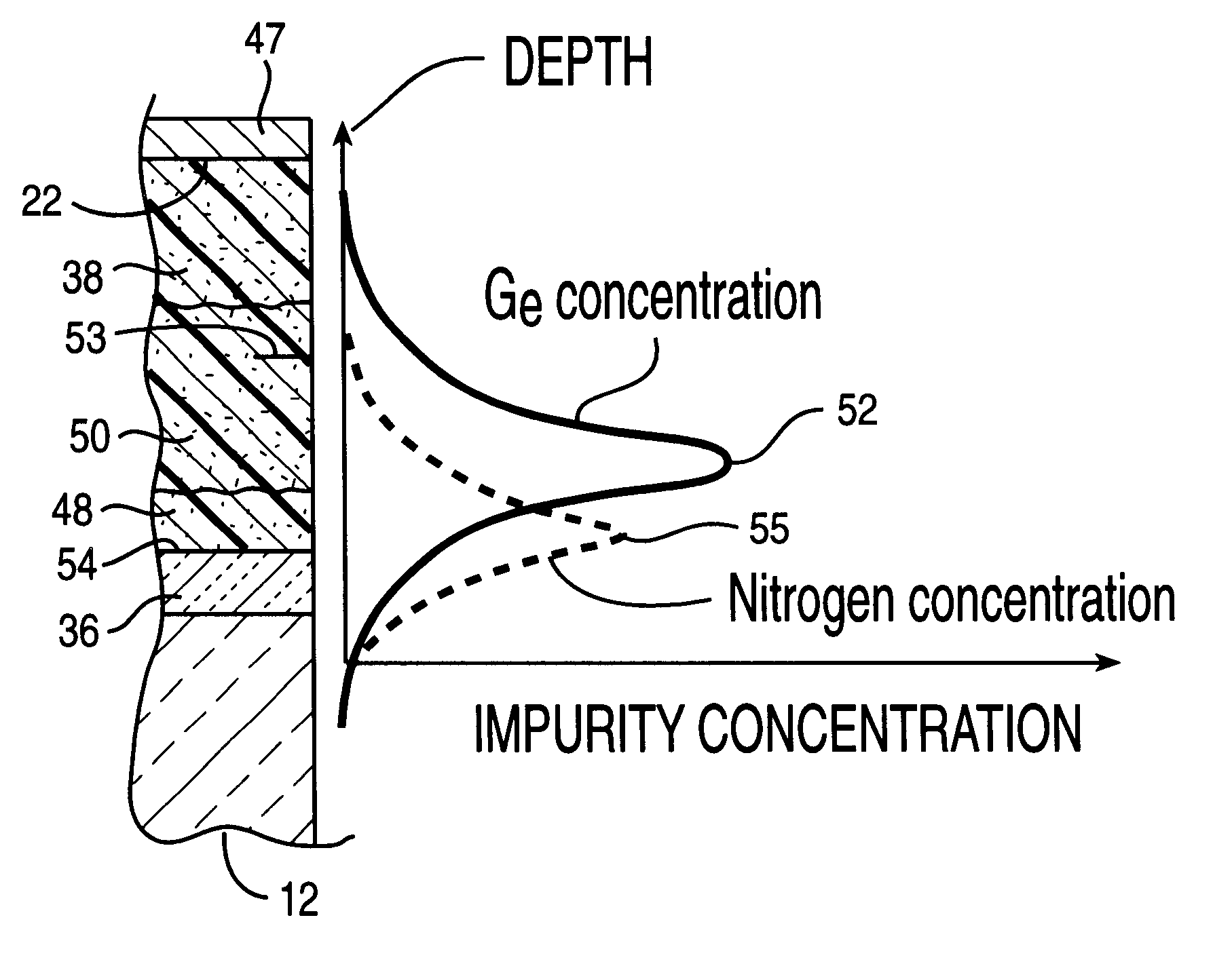
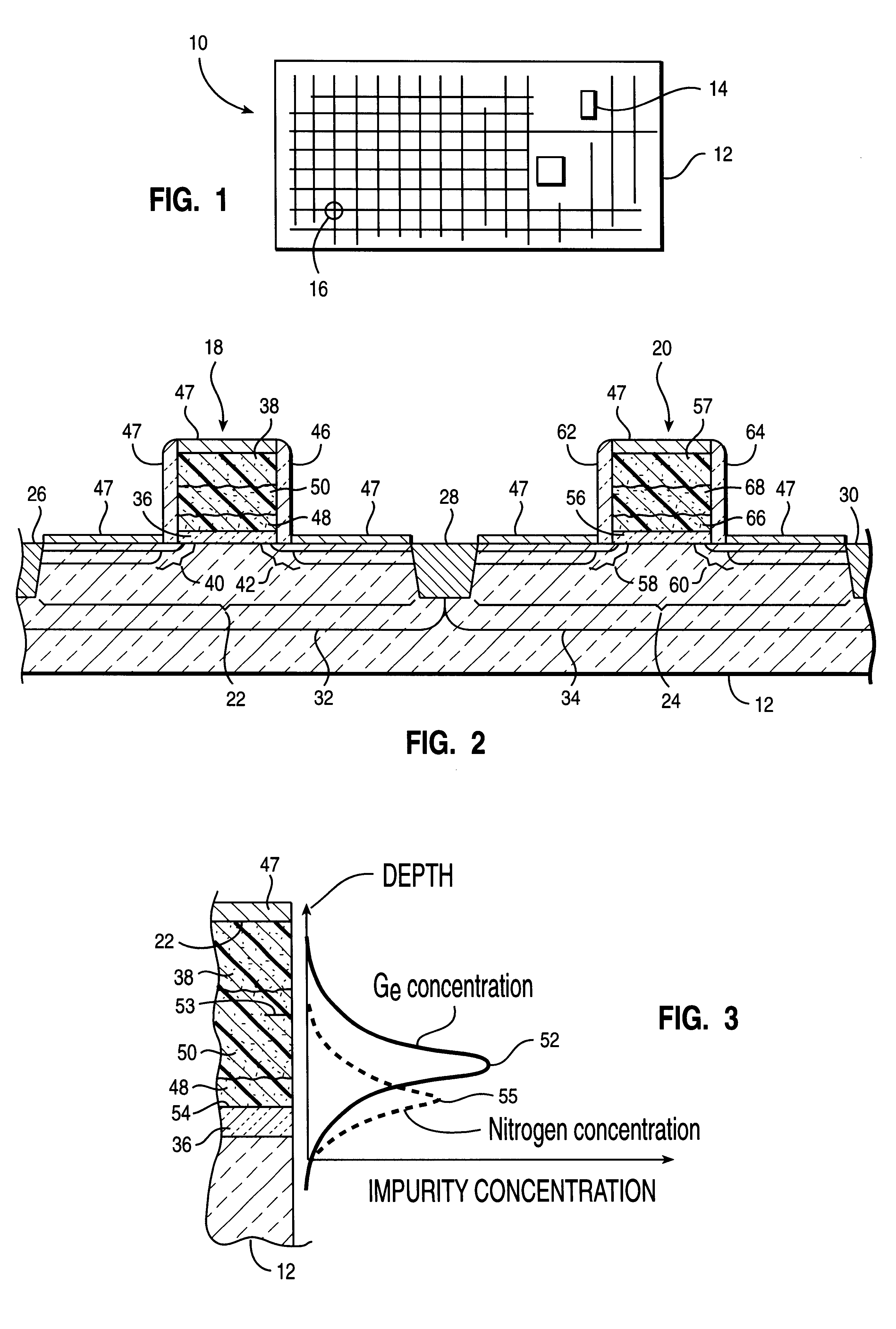
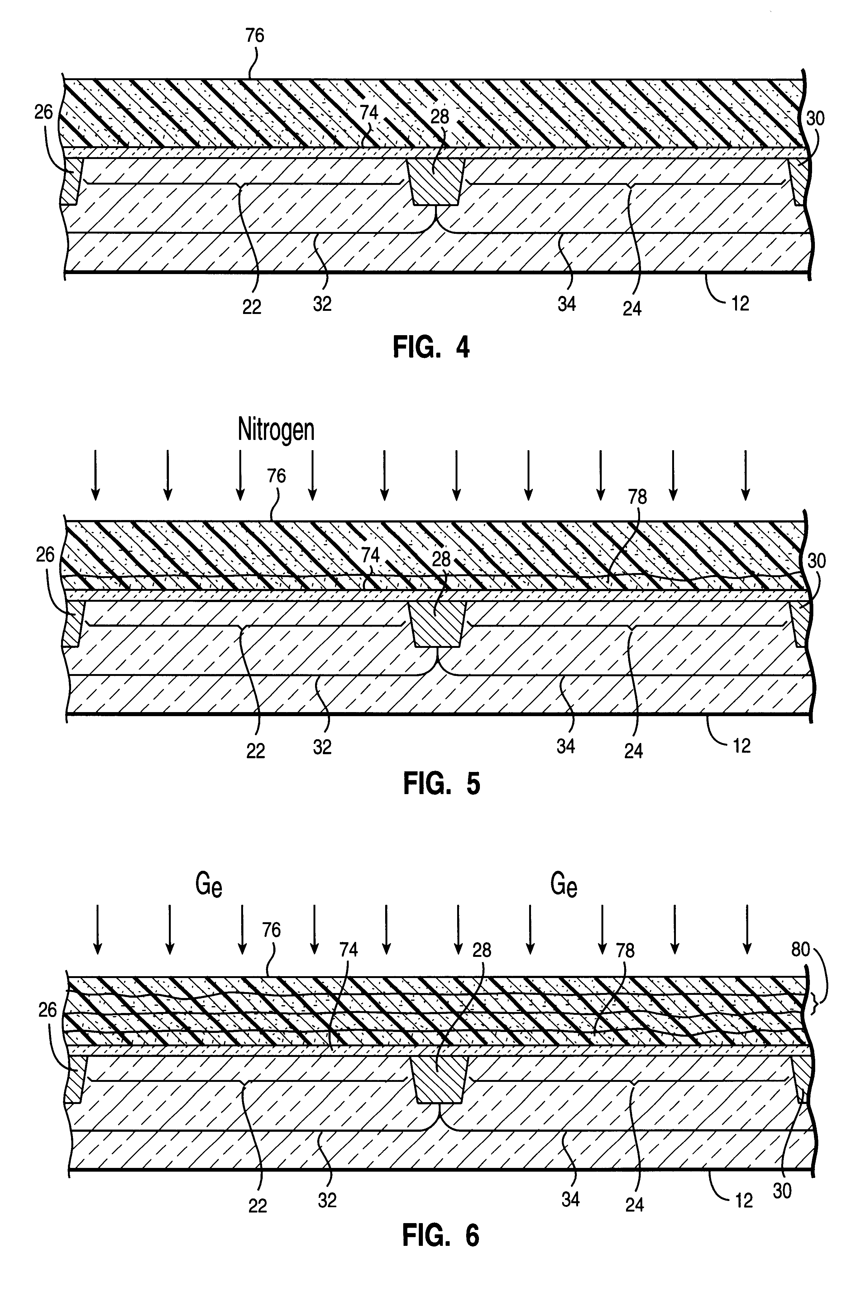
In the drawings described below, reference numerals are generally repeated where identical elements appear in more than one figure. Turning now to the drawings, and in particular to FIG. 1, there is shown a plan view of an exemplary embodiment of an integrated circuit 10 implemented on a semiconductor substrate 12. The integrated circuit 10 includes a plurality of circuit elements depicted schematically and designated 14. The circuit elements 14 include transistors, capacitors, resistors and the like. The substrate 12 may be composed of n-doped silicon, p-doped silicon, silicon-on-insulator, or the like.

The detailed structure of two exemplary transistors of the integrated circuit 10 may be understood by referring now also to FIG. 2, which is a highly magnified cross-sectional view of the portion of the integrated circuit 10 circumscribed by the circle 16 on FIG. 1. The transistors, designated 18 and 20, are implemented on active areas 22 and 24 of the substrate that are circumscribe...


PUM


Abstract

An integrated circuit and a method of making a transistor thereof are provided. In one aspect, the method includes the steps of forming a gate dielectric layer on the substrate and forming a gate electrode on the gate dielectric layer with a lower surface, a midpoint, and a quantity of p-type impurity. A quantity of nitrogen is introduced into the gate electrode whereby the quantity nitrogen has a peak concentration proximate the lower surface. A quantity of germanium is introduced into the gate electrode and first and second source / drain regions are formed in the substrate. The method enables simultaneous formation of n-channel and p-channel gate electrodes with work functions tailored for both types of devices.

Description

1. Field of the InventionThis invention relates generally to semiconductor processing, and more particularly, to an integrated circuit with transistors, and to a method of making the same incorporating a shared doping scheme for transistors of different conductivity types.2. Description of the Related ArtA typical field effect transistor implemented in silicon consists of a source and a drain formed in a silicon substrate, and separated laterally to define a channel region in the substrate. A gate electrode composed of a conducting material, such as aluminum or polysilicon, is disposed over the channel region and designed to emit an electric field into the channel region. Changes in the electric field emitted by the gate electrode enable, or alternatively, disable the flow of current between the source and the drain.In a conventional process flow for forming a typical field effect transistor, a gate oxide layer is grown on a lightly doped silicon substrate and a layer of polysilicon...

Claims


Application Information

Patent Timeline
Patent Type & Authority Patents(United States)
IPC IPC(8): H01L21/02H01L21/28H01L21/70H01L21/8238H01L21/84
CPCH01L21/28035H01L21/823842H01L21/84
Inventor GARDNER, MARK I.KWONG, DIM-LEEHAUSE, FREDERICK N.
Owner GLOBALFOUNDRIES INC
Learn More