Current-induced magnetic switching device and memory including the same

a current-induced magnetic switching and memory technology, applied in the direction of magnetic bodies, instruments, substrate/intermediate layers, etc., can solve the problems of high packing density, cross-talk problems upon the increase of memory density, and conventional structures and methods that do not allow for high packing density

Inactive Publication Date: 2001-07-03
INT BUSINESS MASCH CORP
View PDF12 Cites 639 Cited by
  • Summary
  • Abstract
  • Description
  • Claims
  • Application Information

AI Technical Summary

Benefits of technology

Another object is to provide a write-operation that allows for high packing density without cross-talk.
A further object is to provide a structure in which simpler driving circuits are employed.
Thus, with the unique and unobvious structure and technique of the present invention, the invention is optimized for small magnetic memory structures where magnetic switching thresholds are more stable than the conventional techniques. Further, high packing density without cross-talk is achieved. Moreover, simpler driving circuits may be employed with the invention as compared to the conventional structures and techniques.

Problems solved by technology

The conventional way of write-addressing has been to use an x-y cross-current excitation, which requires large write current, demands stringent magnetic switching characteristic from the memory element, and has cross-talk problems upon the increase of memory density.
Further, the conventional structures and methods do not allow for high packing density without cross-talk.
Further, the driving circuits become complex due to the x-y selective magnetic-field induced write operation.
Thus, conventional magnetic random access memory (RAM) requires read-write operations on small ferromagnetic elements, and have many problems.
However, such a proposal was strictly theoretical.
However, such a model was strictly hypothetical.
Band calculations show that their minority band has a very low carrier concentration, making it prone to disorder-induced localization.
However, the observed transport characteristics do not resemble a clean metal-insulator-metal tunneling junction.

Method used


Image

  • Current-induced magnetic switching device and memory including the same
  • Current-induced magnetic switching device and memory including the same
  • Current-induced magnetic switching device and memory including the same

Examples


Embodiment Construction

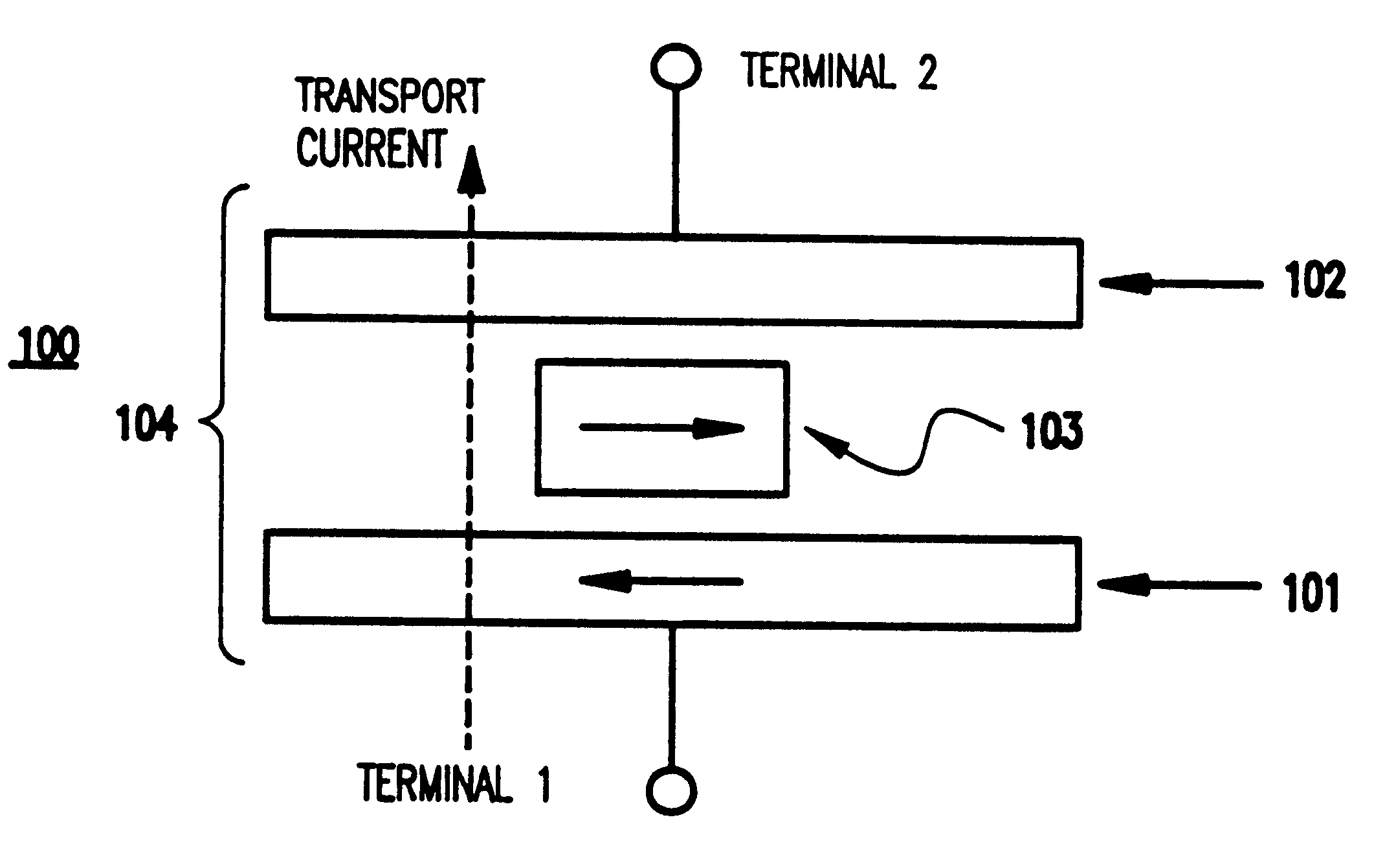
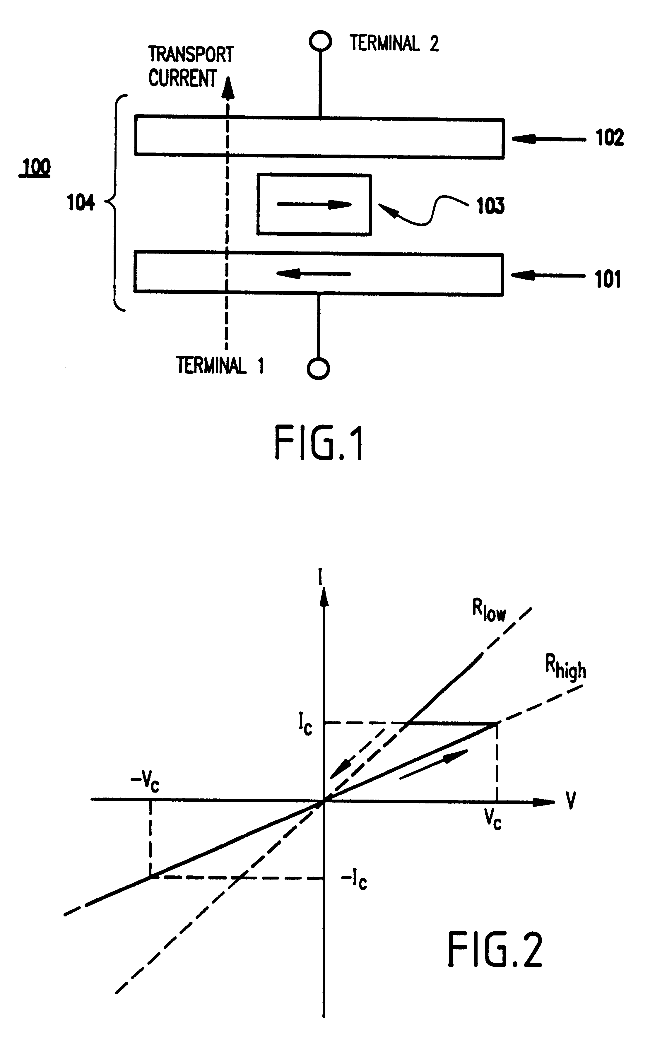
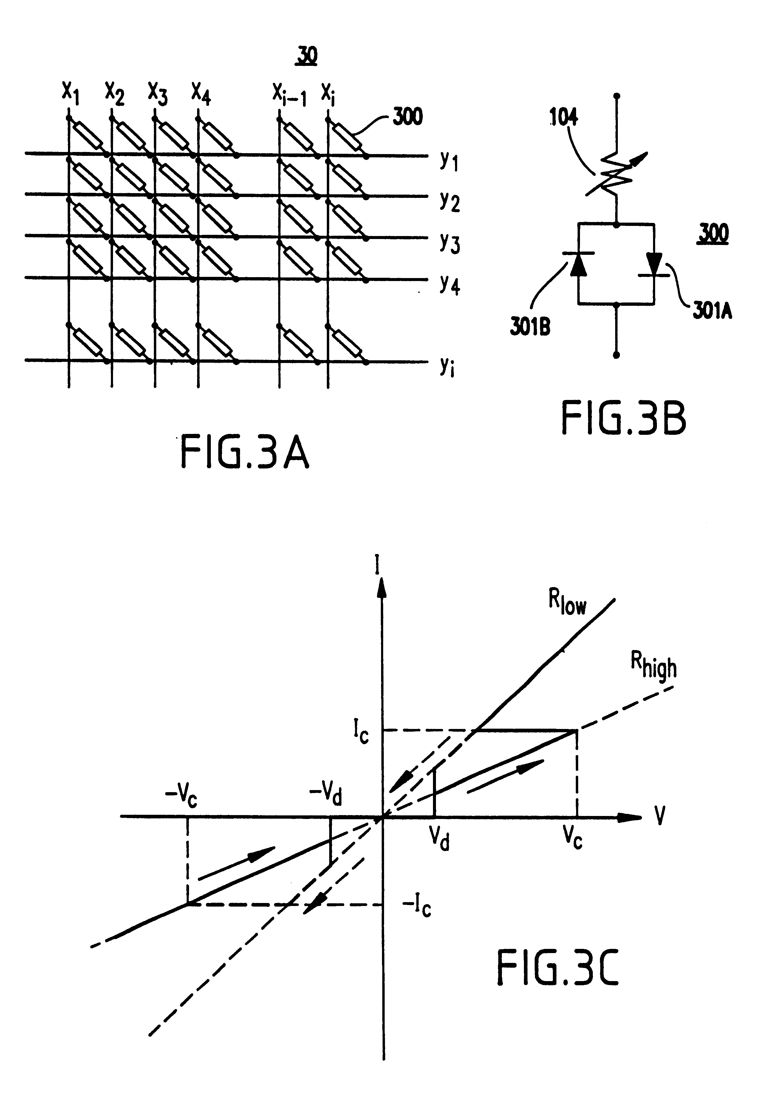
Referring now to the drawings, and more particularly to FIGS. 1-3C, there is shown a preferred embodiment of the present invention.

Generally, the present invention improves upon the conventional devices in terms of the read / write operation and other operations. The present invention is based on momentum transfer from spin-polarized conduction carriers. The technique and structure of the present invention are intrinsically optimal for small magnetic memory structures, where magnetic switching thresholds are more stable. The invention allows extremely high packing density without cross-talk. Further, the invention and its objectives are achieved by simpler driving circuits than the current architecture of an x-y selective magnetic-field induced write.

The invention has been verified by experimental results which verify the quantitative model and finds especially great benefit in a magnetic RAM architecture for a new magnetic memory element, and which are discussed in regard to FIGS. 4-...


PUM

PropertyMeasurementUnit
transport currentaaaaaaaaaa
sizeaaaaaaaaaa
thickaaaaaaaaaa

Abstract

A magnetic switching device, includes a first electrode, a second electrode, and a nanoparticle having a magnetic moment and being disposed between the first and second electrodes. At least one of the first electrode and the second electrode includes a magnetic material which has a net spin polarization in its conduction band for injecting, into the nanoparticle, an electrical current including a net spin polarization for overcoming the magnetic moment of the nanoparticle upon selection of a predetermined magnitude for the electrical current.

Description

1. Field of the InventionThe present invention generally relates to a switching device, and more particularly to a current-induced magnetic switching device for use with a nonvolatile memory array that uses magnetic memory elements as the individual memory cells.2. Description of the Related ArtMagnetic random access memory (MRAM or typically referred to as "MagRam") technology is a solid state device technology using magnetic thin film elements as a storage mechanism. The storage mechanism relies on the relative orientation of the magnetization of two electrodes, and on the ability to discern this orientation by electrical means.MRAM arrays include an array of magnetic memory cells positioned at the intersections of wordlines and bitlines. Generally, each cell includes a magnetically changeable or "free" region, and a proximate magnetically reference region, arranged into a magnetic tunnel junction ("MTJ") device (e.g., the term "reference region" is used broadly herein to denote a...

Claims


Application Information

Patent Timeline
Patent Type & Authority Patents(United States)
IPC IPC(8): H01F10/32G11C11/16G11C11/02H01F10/00H01L43/08
CPCB82Y25/00G11C11/16H01L43/08H01F10/3227H01F10/3254H01F10/3213H10N50/10
Inventor SUN, JONATHAN ZANHONG
Owner INT BUSINESS MASCH CORP
Why Eureka
Try Eureka