Methods and systems for determining chemical concentrations and controlling the processing of semiconductor substrates

Inactive Publication Date: 2001-07-17
CFMT +1
View PDF48 Cites 39 Cited by
  • Summary
  • Abstract
  • Description
  • Claims
  • Application Information

AI Technical Summary

Benefits of technology

The methods and systems of the present invention described are advantageous in that repeated chemical concentration measurements of the same wet processing stream is not required. Instead, a single chemical concentration calculation is performed based on flow rate measurements that provide accurate chemical concentration information that can be used to control the wet proces

Problems solved by technology

A common problem encountered in the wet processing of semiconductor substrates is obtaining repeatable processing results (i.e. process control) for all surfaces of a single semiconductor substrate, between semiconductor substrates in a single batch, and between batches of semiconductor substrates that are processed in the same manner.
However, the use of monitor semiconductor substrates can be costly.
For example, the use of monitor semiconductor substrates leads to lost production time as well as wasted raw materials in processing the monitor semiconductor substrates.
While solution temperature and processing time can readily be controlled in most wet processing systems, the measuring and controlling of chemical concentrations has been problematic.
However, even in an open bath system, in-situ monitors, may not accurately measure chemical concentrations.
For example, when there is more than one chemical present, one may not be able to accurately measure the concentration of a chemical (such as a weak acid or base) due to the presence or interaction of other chemicals (such as a strong acid or strong bas

Method used


Image

  • Methods and systems for determining chemical concentrations and controlling the processing of semiconductor substrates
  • Methods and systems for determining chemical concentrations and controlling the processing of semiconductor substrates
  • Methods and systems for determining chemical concentrations and controlling the processing of semiconductor substrates

Examples


Example

Example

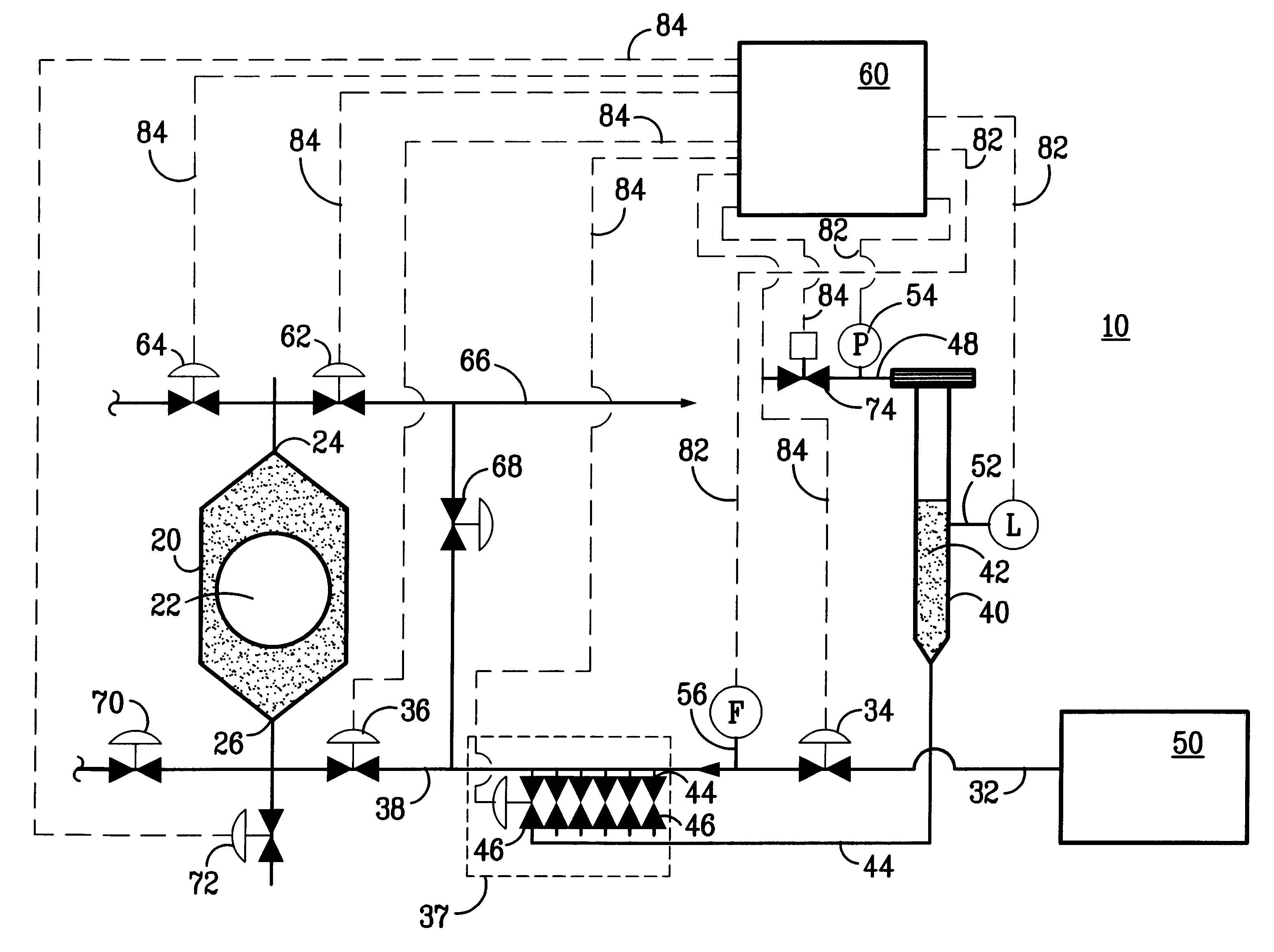
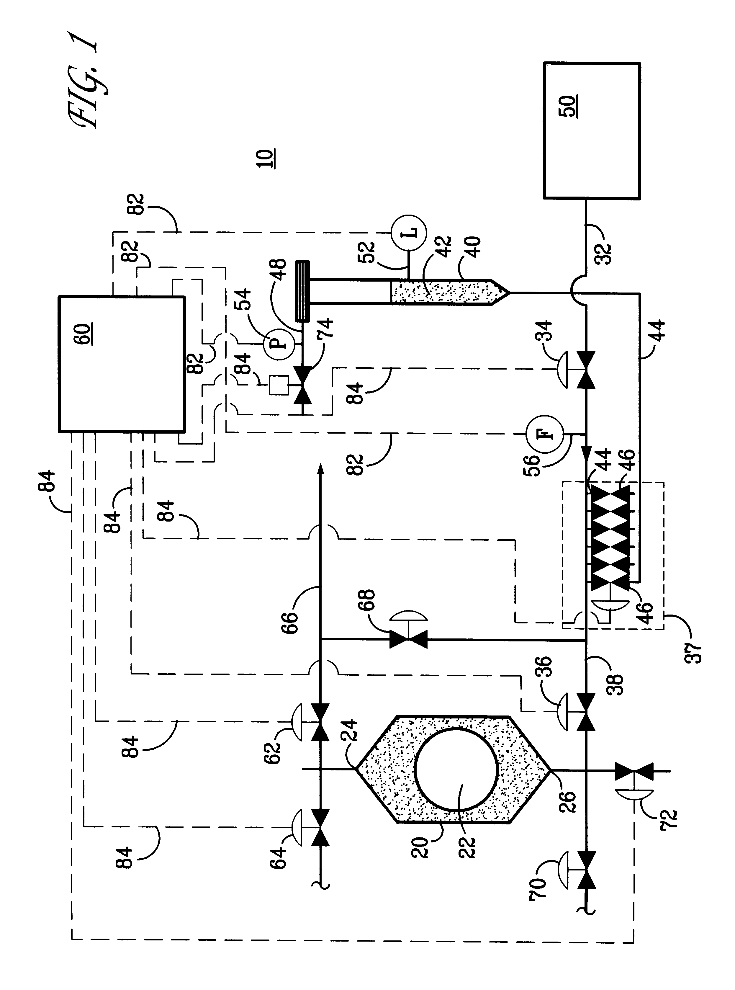
A CFM Full-Flow.TM. system Model No. 8100 was fully loaded with 8" diameter wafers. The equipment set-up was similar to that shown in FIG. 1 to etch the wafers with a hydrofluoric acid solution. The system used included separate liquid supply systems for deionized water and concentrated 49 wt % hydrofluoric acid. The system also had an Alan Bradley PLC processor for receiving flow rate data for the liquid streams.

The wafers were first contacted with deionized water at a flow rate of 18 gpm and temperature of 40.degree. C. for 5 minutes to wet the wafers. After wetting the wafers, a hydrofluoric acid wet processing stream was formed by injecting at a predetermined flow rate 49 wt % concentrated hydrofluoric acid solution into a deionized water stream flowing at a rate of 18 gpm per min. The concentrated hydrofluoric acid was held in a container having a cross sectional area of 18 cm.sup.2 and was injected into the stream of deionized water through the use of nitrogen pressure....


PUM


Abstract

The present invention provides systems and methods of determining the concentration of chemicals in a wet processing stream where the wet processing stream is formed from two or more liquid streams having known chemical concentrations. The concentration of chemicals in the wet processing stream are monitored by measuring the flow rates of the liquid streams during combination to form the wet processing stream, and calculating the concentrations of chemicals in the wet processing stream based on the flow rates and known chemical concentrations of the liquid streams. The present invention also provides systems and methods for controlling the wet processing of semiconductor substrates using the calculated concentrations in the wet processing stream. The methods and systems of the present invention are particularly useful when the semiconductor substrates are contacted with the wet processing stream in a single pass.

Description

The present invention relates to methods and systems for wet processing semiconductor substrates. More particularly, the present invention provides methods and systems for determining chemical concentrations in wet processing streams and controlling the processing of semiconductor substrates.BACKGROUND OF INVENTIONWet processing of semiconductor substrates, such as wafers, flat panels, and other electronic component precursors is used extensively during the manufacture of, for example, integrated circuits. Preferably, wet processing is carried out to prepare the semiconductor substrates for processing steps such as diffusion, ion implantation, epitaxial growth, chemical vapor deposition, and hemispherical silicon grain growth, or combinations thereof. During wet processing, the semiconductor substrates are contacted with a series of process solutions. The process solutions may be used, for example, to etch, to remove photoresist, to clean, or to rinse the semiconductor substrates. S...

Claims


Application Information

Patent Timeline
IPC IPC(8): G01N35/08H01L21/00G01N33/00
CPCG01N35/08H01L21/67086H01L21/67248H01L21/67057G01N2033/0095Y10T436/12
Inventor VERHAVERBEKE, STEVENDIBELLO, GERALD N.MCCONNELL, CHRISTOPHER F.
Owner CFMT
Why Eureka
Try Eureka