CMOS device and circuit and method of operation dynamically controlling threshold voltage

Inactive Publication Date: 2001-08-14
INTELLECTUAL DISCOVERY INC
View PDF15 Cites 41 Cited by
  • Summary
  • Abstract
  • Description
  • Claims
  • Application Information

AI Technical Summary

Problems solved by technology

The variation in threshold voltage of Field Effect Transistors (FET) leads to undesirable effects and limitations in the operating range of integrated circuits.
Modern CMOS technology, while well controlled, can exhibit device threshold voltage (Vth) mismatches in the multi-millivolt range and this can be too much for certain types of circuits to achieve aggressive specifications.
Analog to digital converters of the flash type, comparators, and

Method used


Image

  • CMOS device and circuit and method of operation dynamically controlling threshold voltage
  • CMOS device and circuit and method of operation dynamically controlling threshold voltage
  • CMOS device and circuit and method of operation dynamically controlling threshold voltage

Examples


Embodiment Construction

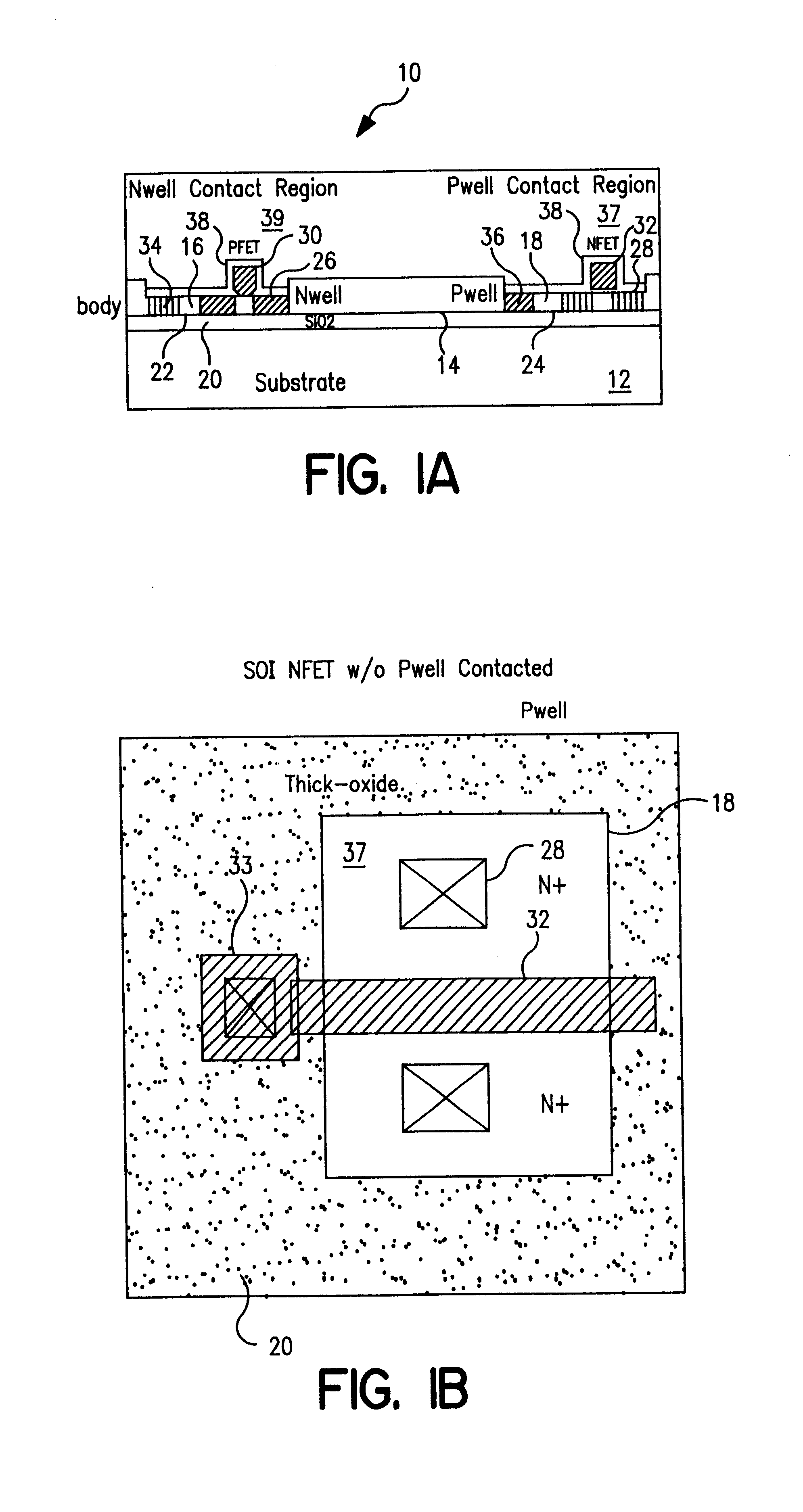
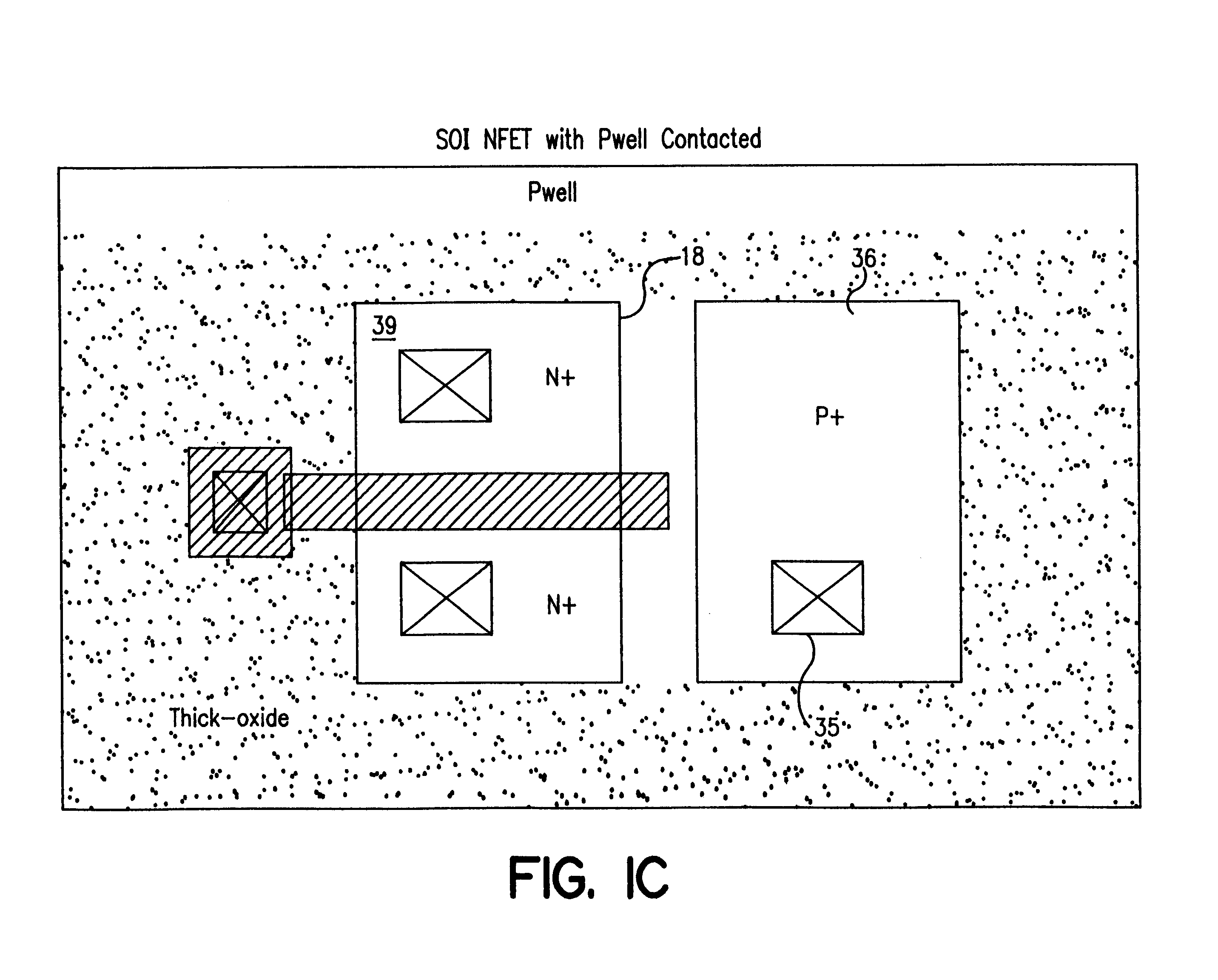
FIG. 1A shows a side view of a CMOS device 10 in silicon-on-insulator technology incorporated in the present invention. The process details of fabricating a silicon-on-insulator device are known in the art and described, for example in U.S. Pat. No. 4,467,518 issued Aug. 28, 1984 assigned to the assigned to the same assignee as that of the present invention and incorporated herein by reference. The device 10 comprises a silicon substrate 12 within which is formed a buried layer of silicon dioxide 14. An n layer 16 and p layer 18 are formed in juxtaposed relation on top of the silicon dioxide layer 14. A thick silicon dioxide layer 20 is formed in the n layer and p layer to establish an n well 22 and a p well 24 separated and surrounded by the thick silicon oxide layer 20. After a region of thin gate oxide is grown over the remaining p well and n well regions, polysilicon gates 30 and 32 are formed over the p well and n well regions. The polysilicon gates and the thick oxide regions ...


PUM


Abstract

A CMOS device fabricated in a silicon-on-insulator structure and including circuitry and methods in a first embodiment dynamically shifts the threshold voltage of the CMOS device in a receiver to provide improved noise margin and in a second embodiment dynamically matches the threshold voltages in a differential amplifier to correct for manufacturing offset. To dynamically shift the threshold voltage for noise immunity, the back gate or bulk nodes of the devices is shifted through two similar circuits comprised of npn inverters with clamping devices. The back gate of the n device is biased at 0 volts for the maximum Vth and is biased at +1 threshold for the minimum Vth of the device. Only the back gate of the p device is biased at Vdd for the maximum Vth of the device and is biased at 1 Vth below Vdd for the minimum Vth of the device. The Vth of the n device and the p device should be less than the forward bias of the respective source volt junctions to prevent unwanted bipolar currents. By driving the back gates in opposite direction and in phase with the input to the receiver circuit, the threshold voltage of the receiver is moved away from ground (GND) when the input is at a logical "0" and way from Vdd when the input is at a logical "1" which raises the noise immunity of the receiver and speeds the response of the receiver to a desired signal To dynamically match a differential pair for offset correction, a feedback circuit performs a Fast Fourier Transformer analysis of the output signal to determine the presence of even harmonics. A feedback voltage is generated representative of the even harmonics and applied to the back bias contacts of the CMOS devices to correct the effects of the threshold mismatch in the differential pair.

Description

1. Field of the InventionThis invention relates to semiconductor devices and circuits and methods of operation. More particularly, the invention relates to apparatus and methods for dynamic control and adjustment of threshold voltage in CMOS devices and circuits.2. Description of Prior ArtThe variation in threshold voltage of Field Effect Transistors (FET) leads to undesirable effects and limitations in the operating range of integrated circuits. Many analog circuits depend on the use of differential pairs of transistors and the threshold matching inherent to those circuits. Modern CMOS technology, while well controlled, can exhibit device threshold voltage (Vth) mismatches in the multi-millivolt range and this can be too much for certain types of circuits to achieve aggressive specifications. Analog to digital converters of the flash type, comparators, and certain types of amplifiers are susceptible to threshold mismatches. Altering the threshold voltage (Vth) of FETs by circuit me...

Claims


Application Information

Patent Timeline
IPC IPC(8): H03K19/00
CPCH03K19/0027H03K2217/0018
Inventor CRANFORD, JR., HAYDEN CLAVIESTEPHENS, GEOFFREY B.
Owner INTELLECTUAL DISCOVERY INC
Why Eureka
Try Eureka