Memory device with multiple processors having parallel access to the same memory area

a memory device and memory area technology, applied in the direction of multi-processing architecture, instruments, program control, etc., can solve the problems of limiting affecting the degree of integration, and occupying the processing elements slightly more than half the chip

Inactive Publication Date: 2001-08-21
SATECH GRP A B LLC
View PDF5 Cites 70 Cited by
  • Summary
  • Abstract
  • Description
  • Claims
  • Application Information

AI Technical Summary

Benefits of technology

FIG. 3 is a simplified logic diagram of decoding circuitry for bit lines an

Problems solved by technology

Due to their complexity, these processing elements take up slightly more than half the chip.
It has been found that yields are low and the cost is expensive.
Locating memory on different chips than the processor elements limits the degree of integration.
The data path between the memory chips and the processors limits the bandwidth available at the sense amplifiers.
However because of the size of the pr

Method used


Image

  • Memory device with multiple processors having parallel access to the same memory area
  • Memory device with multiple processors having parallel access to the same memory area
  • Memory device with multiple processors having parallel access to the same memory area

Examples


Embodiment Construction

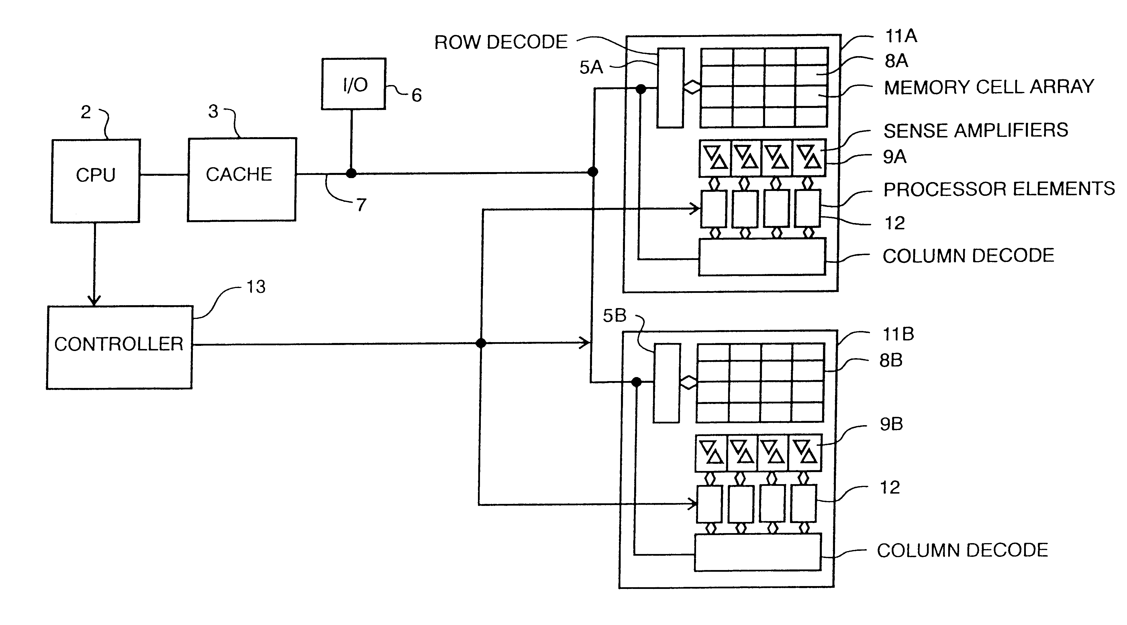
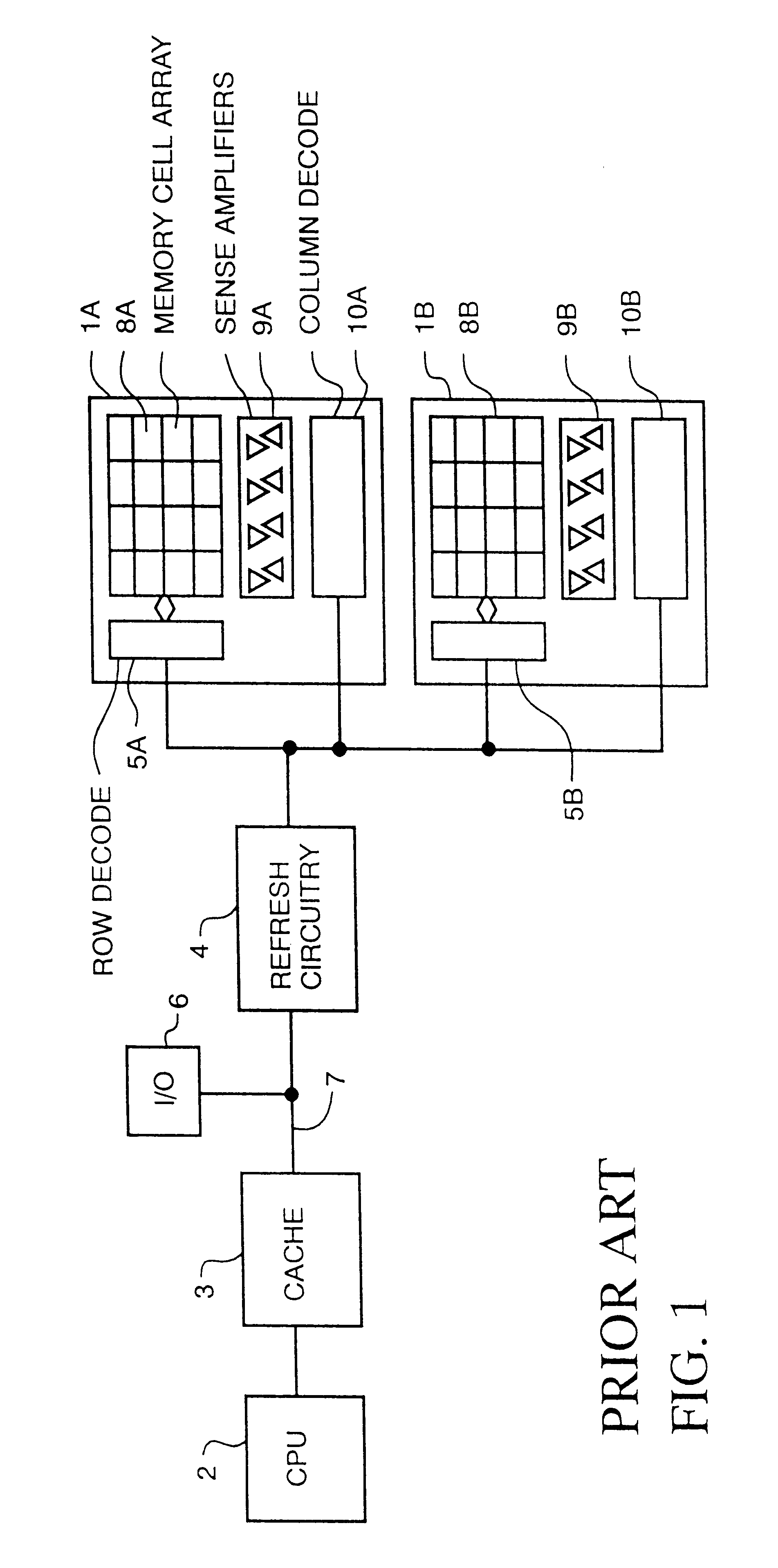
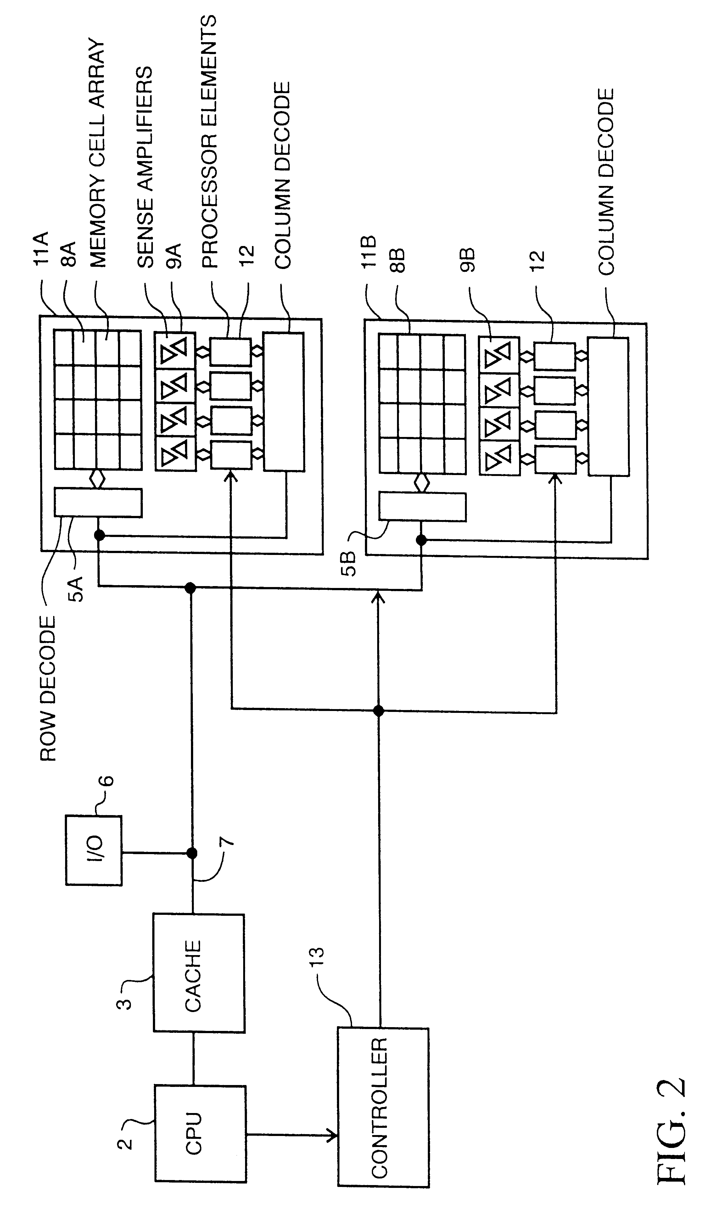
Turning to FIG. 1, a memory comprised of memory portions (chips) 1A and 1B is shown. A central processing unit 2 is connected to a cache memory 3, which is connected to refresh circuitry 4, which is connected to memory address and row decode circuitry 5A and 5B. The computer input / output (I / O) circuit 6 is connected to the address and data bus 7 which is connected to cache 3. Each of the representative memory portions 1A and 1B is comprised of row decode circuitry 5A, 5B, a memory cell array 8A, 8B, sense amplifiers 9A, 9B connected to each column of memory cells, and column decode circuitry 10A, 10B.

In operation, CPU 2 addresses a row and column of a memory cell array in a well known manner, and applies a read enable or write enable signal to the decode circuitry which either reads or stores a bit in a memory cell via the sense amplifiers.

A representative CMOS memory cell is illustrated in FIG. B11 of Microcomputer Primer by Mitchell Waite and Michael Pardee, Howard W. Sams & Co. I...


PUM


Abstract

A digital computer performs read-modify-write (RMW) processing on each bit of a row of memory in parallel, in one operation cycle, comprising: (a) addressing a memory, (b) reading each bit of a row of data from the memory in parallel, (c) performing the same computational operation on each bit of the data in parallel, using an arithmetic logic unit (ALU) in a dedicated processing element, and (d) writing the result of the operation back into the original memory location for each bit in the row.

Description

This invention relates to computer structures, and in particular to a parallel processing memory chip containing single instruction, multiple data path processors.DESCRIPTION OF THE PRIOR ARTIn conventional Von Neumann computer architectures, the speed of the processor is often restricted by the bandwidth of the interconnecting data bus, which is typically 8 to 64 bits in word width. In order to increase the speed of computers restricted by such constraints, parallel computer architectures have been designed, for example, those described briefly below.In a structure called The Connection Machine, 64K processors are used with 4K bits of memory allocated to each processor. The memory permits two read functions and a write function in one processor cycle to support three operand instructions. The Connection Machine integrated circuit chip contains 16 processors and a hypercube routing node. A high performance interconnect network is a major feature of the architecture. The peak perform...

Claims


Application Information

Patent Timeline
IPC IPC(8): G06F15/76G06F15/80G11C7/10
CPCG06F9/30043G06F9/3879G06F9/3887G06F15/7821G11C7/1006G06F15/8015G11C2207/104Y02B60/1225Y02D10/00
Inventor ELLIOTT, DUNCAN G.SNELGROVE, W. MARTIN
Owner SATECH GRP A B LLC
Why Eureka
Try Eureka