
Multiple state electronic device

a multi-state electronic device and electronic device technology, applied in the field of semiconductor devices, can solve the problems of system requirements for complex logic circuitry, the complexity of analog and digital integrated circuit manufacturing seems to be approaching the optical resolution limit, and the difficulty of finding electronic components having incremental multiple stable states

Inactive Publication Date: 2001-09-18
WITMER WARNER HARRY
View PDF3 Cites 1 Cited by
  • Summary
  • Abstract
  • Description
  • Claims
  • Application Information

AI Technical Summary

Benefits of technology

An objective of the inventive device disclosed herein is to provide advanced circuitry architecture for A-to-D conversion with inherently faster response speed and direct applicability to waveform integration and differentiation.
A further goal of the invention is disclosure of applicability of the proposed circuit architecture with enhanced performance, power consumption, circuit density, and potential manufacturing yield compared with conventional binary architectures.
The combined parameters of waveform amplitude detection and the cycle time T allows additional usefulness including differentiation and integration of the waveform. The recurring cycle time period T. corresponding to charge step transfer time for a full cycle, or one revolution of the recurring CCD, allows immediate integration and differentiation using well-known successive approximations. As cycle time becomes faster, the output waveform approaches the waveform integral as a limit by summation of the output values. Similarly, differentiation of the analog waveform is accomplished by dividing the successive difference of output values by the differentiation time. Thereby the waveform output approaches the differentiation limit as cycle time becomes faster. Cycle time can be extremely fast in CCD devices.
A further object of the multistate electronic device is advanced circuitry architecture allowing faster response speed and decreased gate requirements with applicability to integrated data systems by furthering the goal of high performance, low power consumption, high circuit density, and high manufacturing yield compared with conventional binary technologies.
The desirable technical features of the multi-state device are the following (I) much decreased gate complexity for a given numerical expression, (2) high speed by reduced gate requirement, and (3) improved manufacturing yield by decreased gate density.

Problems solved by technology

Especially it has been found extremely difficult to find electronic components having incremental multiple stable states.
However, the semiconductor charge coupled device portion of that system produced only a digital counting representation (unitary based number system) of the input analog signal, and the system required complex logic circuitry to convert this digital counting representation into the ultimately desired representation in the binary number system.
First of all, analog and digital integrated circuit manufacturing complexity seems to be approaching an optical resolution limit whereby it is becoming difficult to increase the number of gates on a chip.
The technical disadvantages of binary-based integrated circuit technology are (1) maximum MOST gate complexity of any number system, (2) slowest speed of any radix system, and (3) decreased manufacturing yield because of the huge number of MOSTs required for number representation.
This is a consequence of inherent signal delay times, each gate.
These conversion processes require many extremely complicated electronic integrated circuits whereby the total binary conversion times, plus delay due to the huge number of binary switching components results in considerable reduction of circuit speed.

Method used


Image

  • Multiple state electronic device
  • Multiple state electronic device
  • Multiple state electronic device

Examples


Embodiment Construction

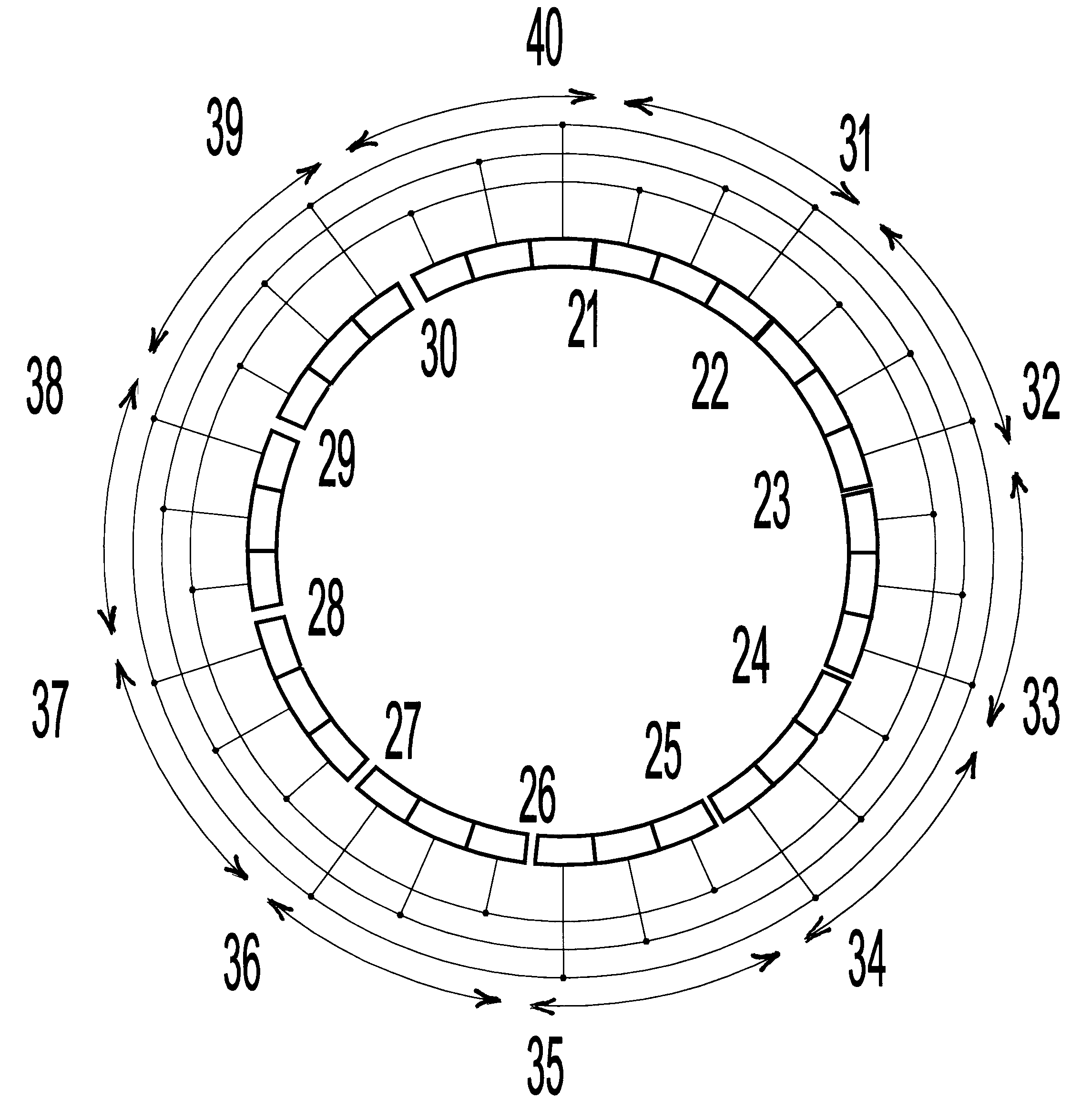
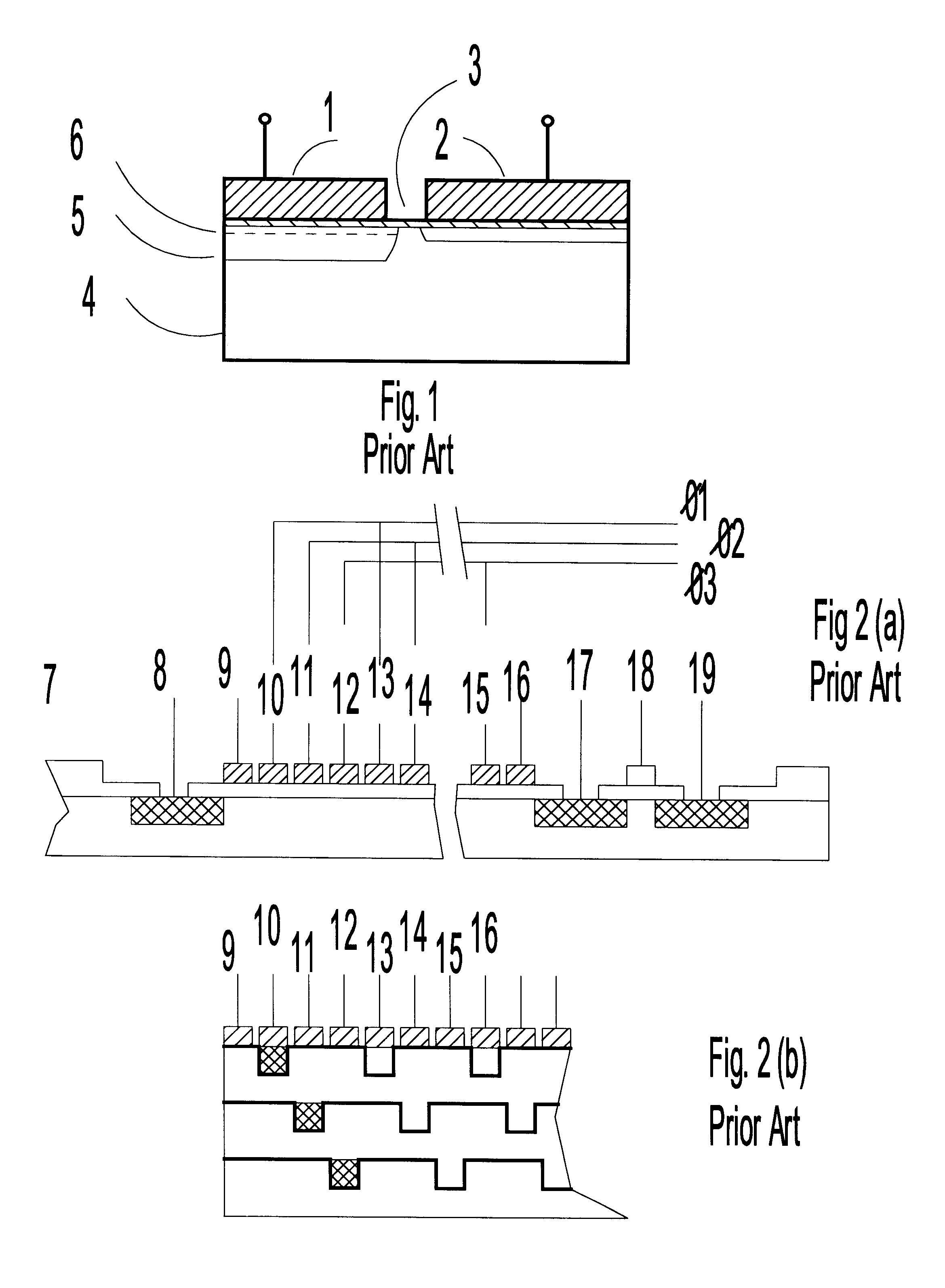
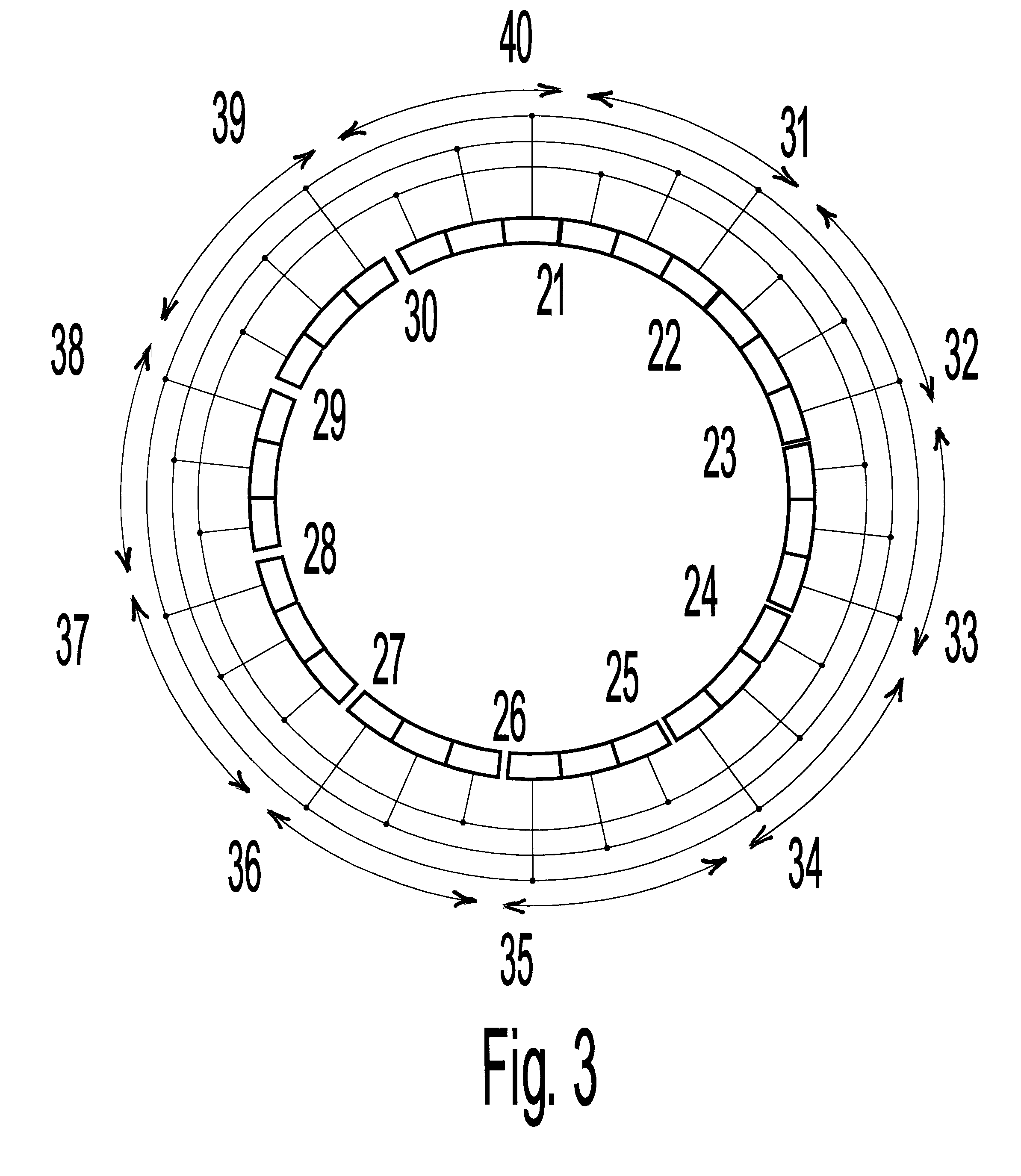
Referring now to FIG. 4 there is shown an embodiment for a recurring three phase 12-state CCD. Electrode groups 43, 44, 45, 46, 47, 48, 49, 50, 51, 52, 53 and 54 are charge transfer stages each including a .O slashed..sub.1 electrode, a .O slashed..sub.2 electrode, a .O slashed..sub.3 `rest` electrode, plus, in common, charge detection gate 59, with associated charge detection diodes each transfer stage. Each charge transfer stage of the recurring device is set by selected distance of the .O slashed..sub.3 `rest` electrode from the succeeding (i.e., clockwise) .O slashed..sub.1 electrode by increasingly higher charge transfer voltage requirement as described previously. In this 12-state CCD configuration ion implantation incrementally applied between successive .O slashed..sub.3 `rest` electrode and succeeding 01 electrode determines the positive voltage required for charge packet transfer thus allowing the charge packet to "rest" allowing pulsing of charge detection gate 59 at conc...


PUM


Abstract

This invention relates to semiconductor apparatus capable of multiple stable electronic states allowing higher order mathematical radix analysis of analog and digital signals. The device accomplishes direct A / D signal conversion with increased circuit speed while decreasing electronic component density compared to computational circuits based on binary conversion. In particular the invention relates to semiconductor apparatus and devices for analog-to-digital conversion and waveform differentiation or integration of electronic signals by use of higher order number systems. In addition the invention relates to novel construction of charge-coupled devices finding applications especially with respect to detection and manipulation of electronic signals for A / D conversion, mathematical differentiation, integration, and encryption of electronic waveform signals.

Description

1. Field of the InventionThis invention relates to semiconductor apparatus capable of multiple stable electronic states allowing higher order mathematical radix analysis of analog and digital signals. In particular the invention relates to semiconductor apparatus and devices for analog-to-digital conversion and waveform differentiation or integration of electronic signals by use of higher order number systems. The invention discloses construction of semiconductor charge coupled devices for accomplishing the same. In addition the invention relates to novel construction of charge-coupled devices finding applications in electronics, especially with respect to detection and manipulation of electronic signals for A / D conversion, mathematical differentiation, and integration of electronic waveform signals. The device accomplishes direct A / D signal conversion with increased circuit speed while decreasing electronic component density compared to computational circuits based on binary conver...

Claims


Application Information

Patent Timeline
Patent Type & Authority Patents(United States)
IPC IPC(8): H03M1/34H03M1/12
CPCH03M1/34H03M1/1235
Inventor WITMER, WARNER HARRY
Owner WITMER WARNER HARRY
Learn More