Stackable ceramic FBGA for high thermal applications

a technology of high-temperature thermal applications and stackable ceramics, which is applied in the direction of electrical equipment, semiconductor devices, semiconductor/solid-state device details, etc., can solve the problems of increased heat generated during operation, and achieve the effect of minimizing lead length and high operating speed

Inactive Publication Date: 2001-10-02
MICRON TECH INC
View PDF57 Cites 257 Cited by
  • Summary
  • Abstract
  • Description
  • Claims
  • Application Information

AI Technical Summary

Benefits of technology

However, as the speed of the semiconductor die increases, the heat generated during operation increases. Additionally, it becomes necessary to shorten the leads between the printed circuit board on which the IC is located and the IC device itself in order to keep the impedance of the circuit from affecting the response speed of the IC device.
Therefore, a packaging is required for semiconductor dice which have high operating speeds and generate heat associated therewith while minimizing the lead length between the semiconductor dice and the printed circuit boards on which they are mounted.

Problems solved by technology

However, as the speed of the semiconductor die increases, the heat generated during operation increases.

Method used


Image

  • Stackable ceramic FBGA for high thermal applications
  • Stackable ceramic FBGA for high thermal applications
  • Stackable ceramic FBGA for high thermal applications

Examples


Embodiment Construction

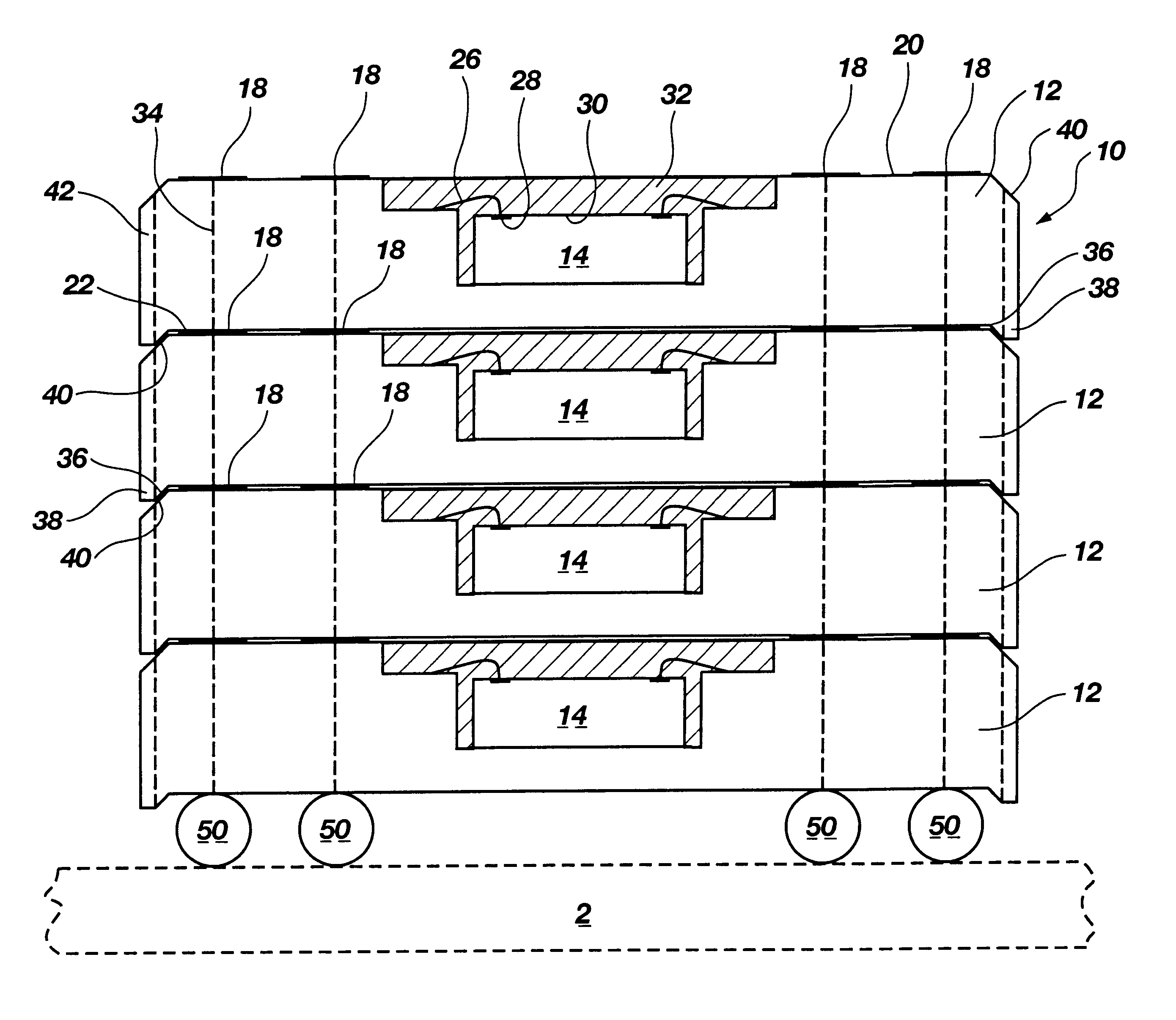
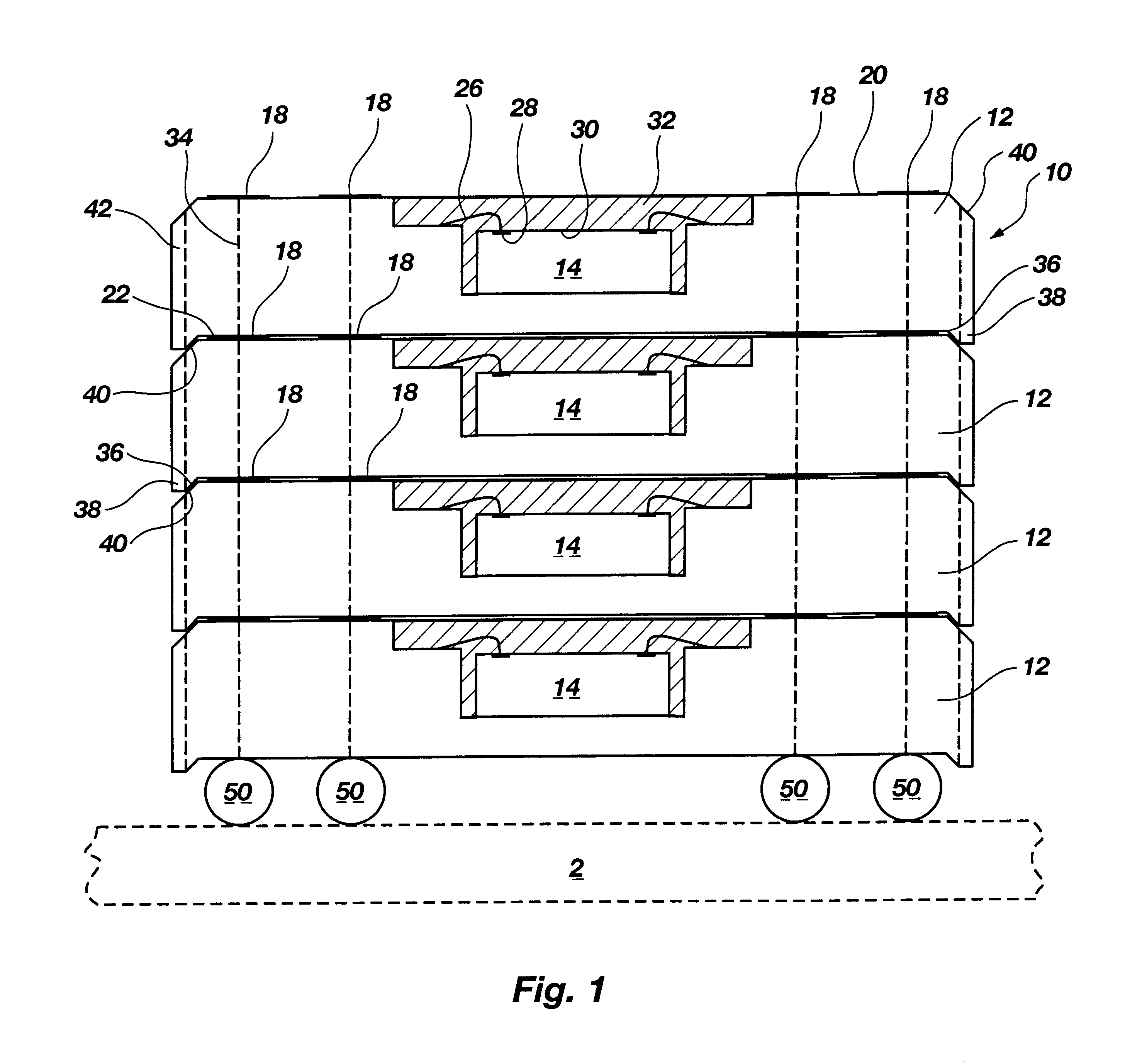
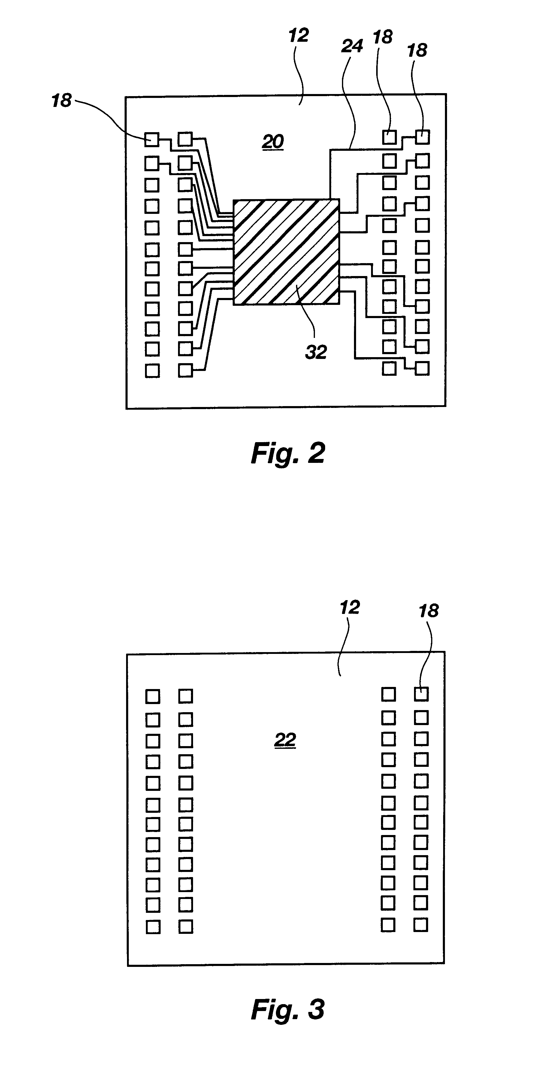
Referring to drawing FIG. 1, a plurality of assemblies 10 comprising a carrier 12 and a semiconductor device 14 located therein is illustrated installed on a substrate 2. Each carrier 12 comprises a member having a cavity 16 therein. As illustrated, the cavity 16 may be a single level or multi-level cavity having any desired number of levels therein. The carrier 12 is formed having a plurality of contact pads 18 located on the upper surface 20 and lower surface 22 thereof which is connected by circuits 24 (not shown) and by wire bonds 26 to the bond pads 28 located on the active surface 30 of the semiconductor die or device 14. The semiconductor die or device 14 is initially retained within the cavity 16 by any suitable means, such as adhesive, etc. The circuits 24 (not shown) are formed on the upper surface 20 of the carrier 12 and portions of the walls or surfaces of the cavity 16 by any suitable well known means, such as deposition and etching processes. The wire bonds connecting...


PUM

PropertyMeasurementUnit
semiconductoraaaaaaaaaa
temperatureaaaaaaaaaa
electricallyaaaaaaaaaa

Abstract

An apparatus package for high temperature thermal applications for ball grid array semiconductor devices and a method of packaging ball grid array semiconductor devices.

Description

1. Statement of the InventionThe present invention relates to an apparatus for high-temperature thermal applications for ball grid array semiconductor devices and a method of packaging ball grid array semiconductor devices.2. State of the ArtIntegrated semiconductor devices are typically constructed in wafer form with each device having the form of an integrated circuit die which is typically attached to a lead frame with gold wires. The die and lead frame are then encapsulated in a plastic or ceramic package, which is then commonly referred to as an integrated circuit (IC). ICs come in a variety of forms, such as a dynamic random access memory (DRAM), static random access memory (SRAM), read only memory (ROM), gate arrays, etc. The ICs are interconnected in many combinations on printed circuit boards by a number of techniques, such as socketing and soldering. Interconnection among ICs arrayed on a printed circuit board are typically made by conductive traces formed by photolithogra...

Claims


Application Information

Patent Timeline
Patent Type & Authority Patents(United States)
IPC IPC(8): H01L23/12H01L23/13H01L25/10
CPCH01L23/13H01L25/105H01L23/3128H01L2224/16H01L2224/48091H01L2224/48227H01L2225/0651H01L2225/06517H01L2225/06541H01L2225/06572H01L2225/06586H01L2924/01079H01L2924/15153H01L2924/15165H01L2924/1517H01L2924/15173H01L2924/15311H01L2924/15331H01L2924/3011H01L2924/00014H01L24/48H01L2924/01087H01L2224/45144H01L2924/00H01L2224/32225H01L2224/73265H01L2225/1058H01L2924/00012H01L24/45H01L24/73H01L2924/14H01L2924/1627H01L2924/00015H01L2224/05599
Inventor MODEN, WALTER L.CORISIS, DAVID J.MESS, LEONARD E.KINSMAN, LARRY D.
Owner MICRON TECH INC
Why Eureka
Try Eureka