

Light shielding structure of a substrate for a liquid crystal device, liquid crystal device and projection type display device
a technology of liquid crystal devices and substrates, applied in static indicating devices, instruments, non-linear optics, etc., can solve problems such as leakage current to flow, leakage current generated by exposure of tft to stray light, and leakage current to aris
- Summary
- Abstract
- Description
- Claims
- Application Information
AI Technical Summary
Benefits of technology
Problems solved by technology
Method used
Image

Examples
embodiment 1
(Embodiment 1)
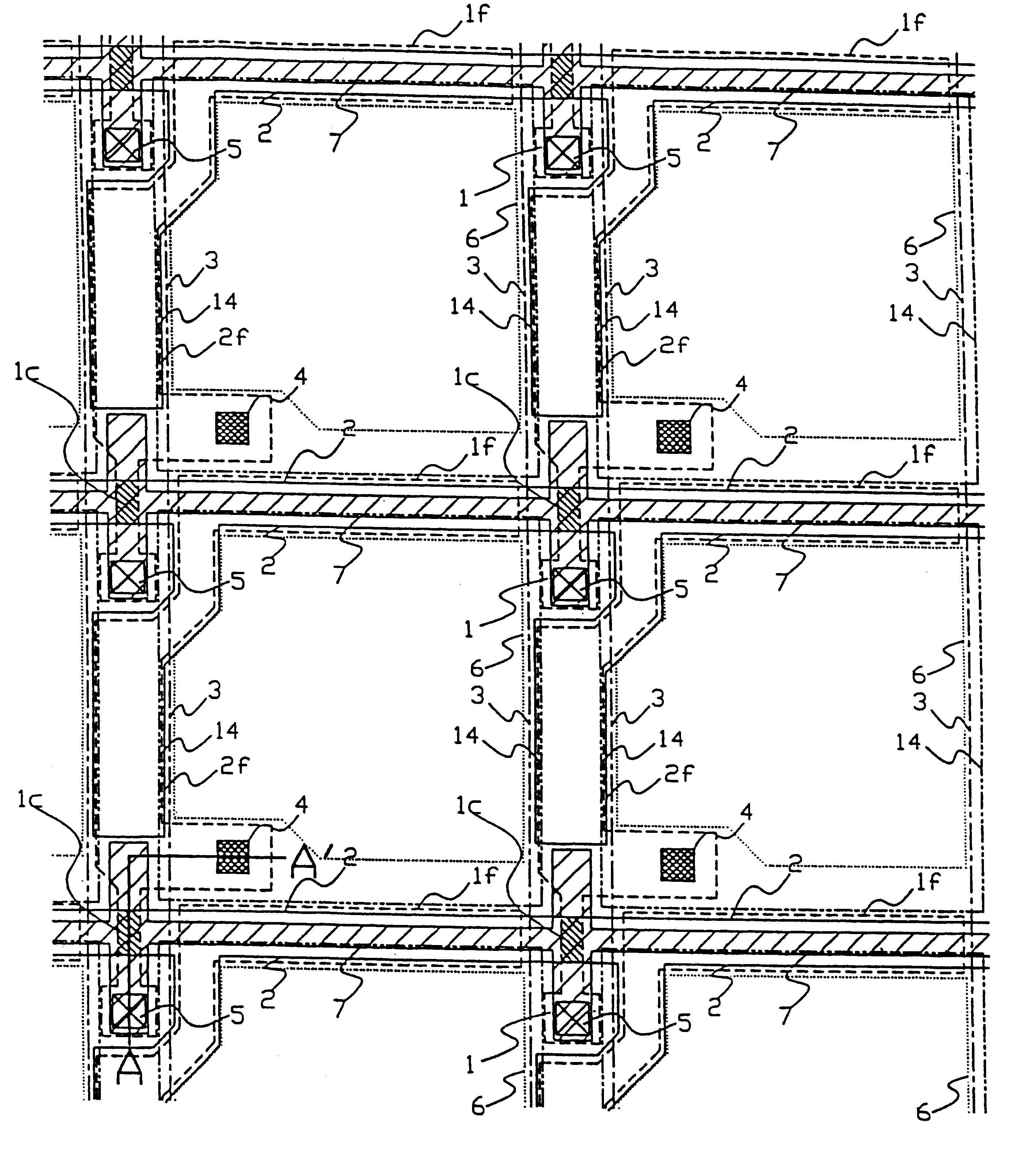
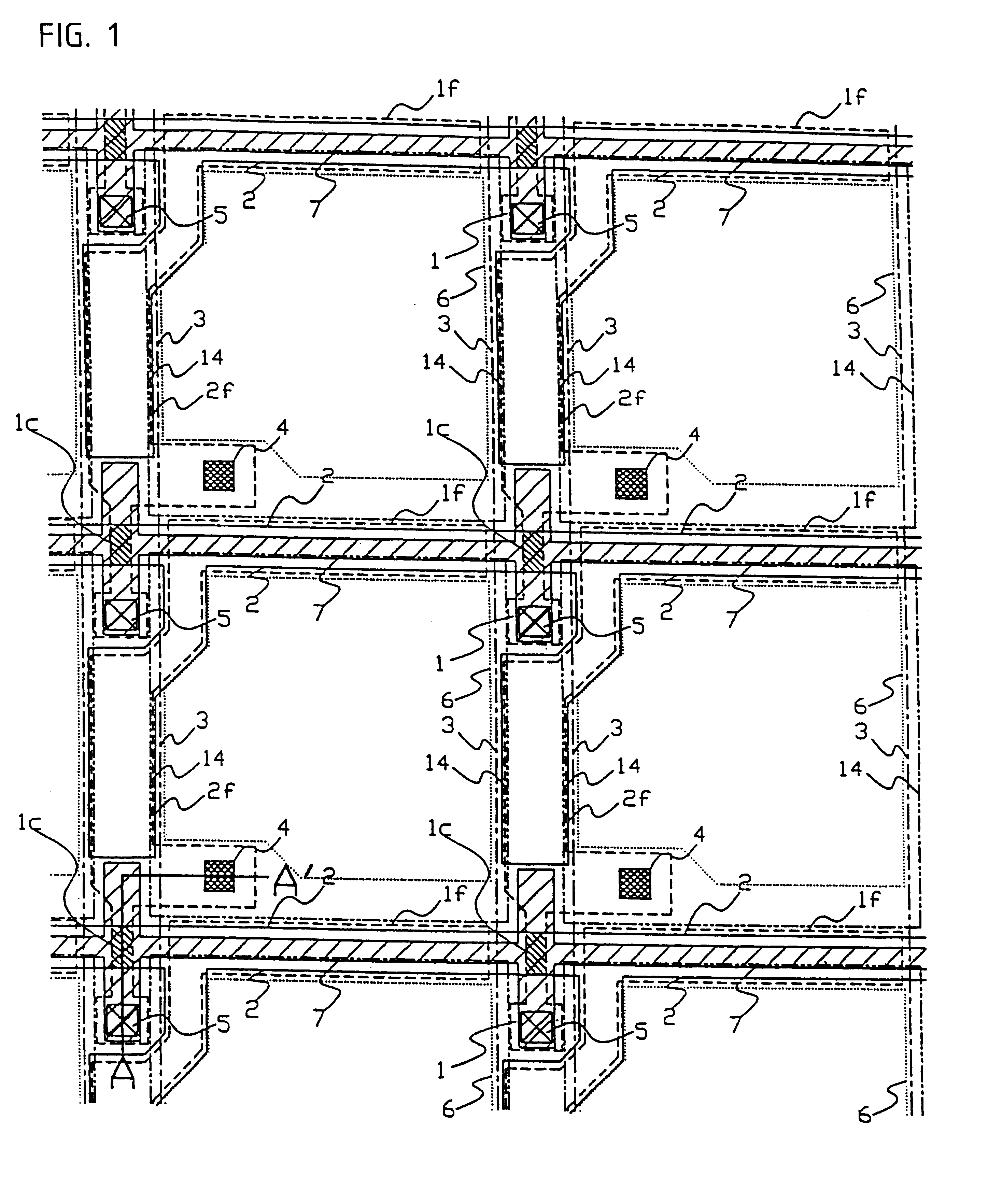
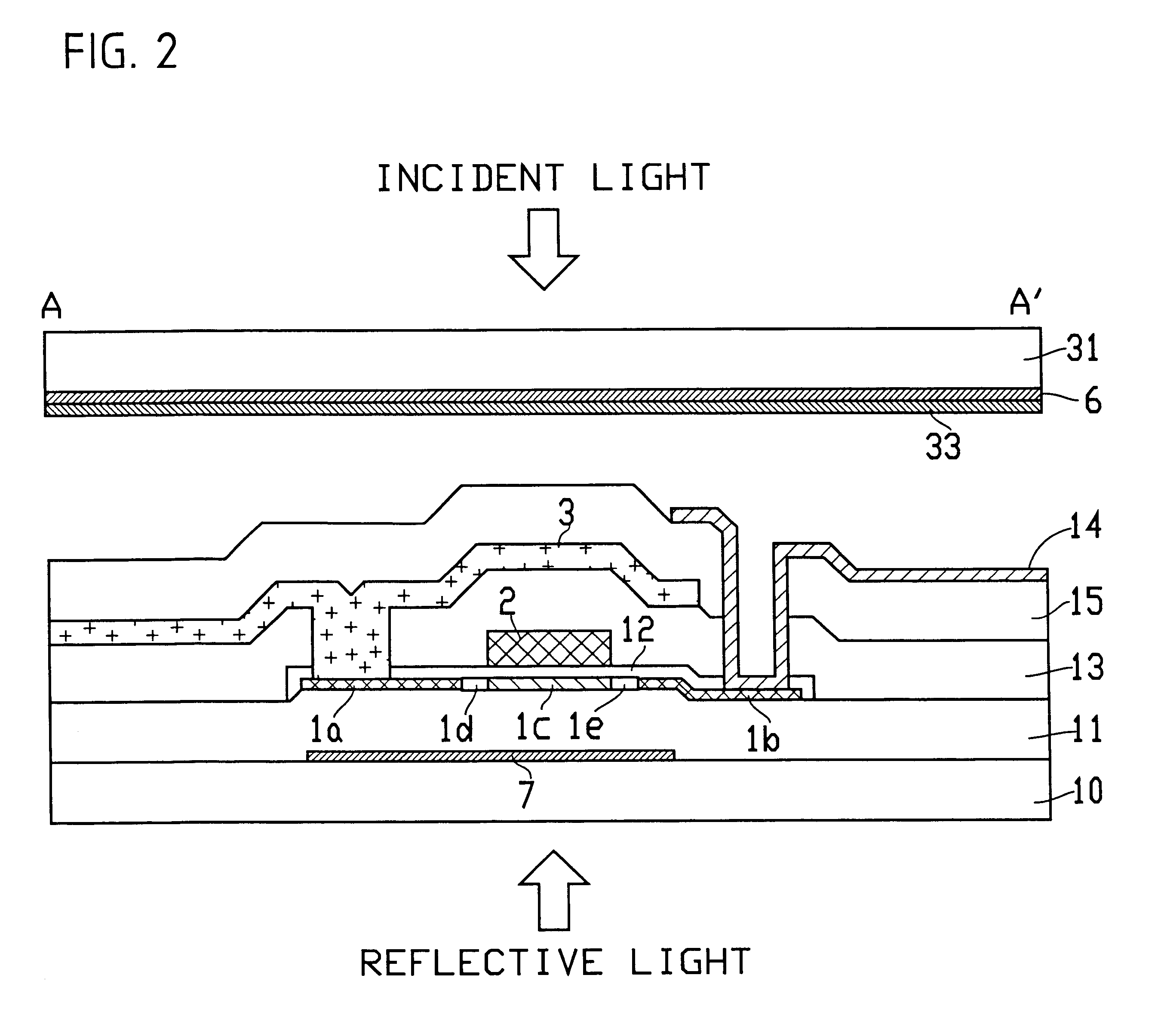
FIGS. 1 and 2 represent the first preferred embodiment of a substrate for a liquid crystal device to which this invention has been applied. FIG. 1 is a plan view of pixels arrayed side by side, while FIG. 2 is a sectional view of the same along line A-A' of FIG. 1, that is, a cross-section of a semiconductor layer 1 which serves as an active layer of a TFT.
In FIG. 1. 1 represents a polysilicon film which forms a first layer of the semiconductor layer of the TFT, and, on the surface of semiconductor layer 1 is formed a gate insulating film 12 which has been produced by thermal oxidation, as shown in FIG. 2. Scan lines 2 act as common gate electrodes to TFTs arrayed in the same column (arrayed crosswise in the figure), 3 represents a data line which is so placed lengthwise as to intersect the scan line 2 at right angles, and is introduced to provide a voltage to the source regions of the TFTs arrayed in a vertical direction along the same row. The scan line 2 is made of ...
embodiment 2
In embodiment 2 like embodiment 1, the first light shielding film 7 is prepared smaller in size than a black matrix formed on an opposite substrate 31. Accordingly, incident light is prevented from impinging directly on the surface of first light shielding film 7, and thus generation of leakage current due to light reflected from the first light shielding film 7 can be effectively suppressed. Further, the first light shielding film 7 is so prepared as to have a smaller width than does the scan line 2, thereby preventing direct impingement of incident light on the first light shielding film 7 which extends below the scan line 2 in the same direction.
In embodiment 1, though not being restrictive, to effectively confer an extra capacitance to the drain of the TFT, the channel region 1c of the first layer of semiconductor layer 1 takes a course as indicated by symbol 1f: it extends above along the data line 3, and flexes towards an adjacent pixel electrode 14 (of the left adjacent pixel...
embodiment 3
can also be produced through the same production processes as used for the production of embodiment 1.
(Embodiment 4)
FIGS. 9 and 10 represent the fourth preferred embodiment of a substrate for liquid crystal device to which this invention has been applied. FIG. 9 is a plan view of pixels arrayed side by side, while FIG. 10 is a sectional view of the same along line D-D' of FIG. 9, that is, a cross-section of a semiconductor layer 1 which serves as an active layer of the TFT. Embodiment 4 differs from embodiment 3 in that a scan line 2 has a laminated structure consisting of a polysilicon layer 2a and a metal film such as a tungsten film, a molybdenum film, etc., or a metal alloy film 2b, and in that the first light shielding film 7 (areas shaded with parallel lines having a positive gradient) is place only below a data line 3 (second light shielding film). In embodiment 3 described above, as a polysilicon film constituting the scan line 2 alone is present above the first light shield...
PUM
| Property | Measurement | Unit |
|---|---|---|
| distance | aaaaa | aaaaa |
| distance L1 | aaaaa | aaaaa |
| distance L2 | aaaaa | aaaaa |
Abstract
Description
Claims
Application Information