Semiconductor memory device
a memory device and semiconductor technology, applied in semiconductor devices, digital storage, instruments, etc., can solve the problems of tft transistor formation, difficult to ensure the precision of read data, small read signal,
- Summary
- Abstract
- Description
- Claims
- Application Information
AI Technical Summary
Problems solved by technology
Method used
Image

Examples
first embodiment
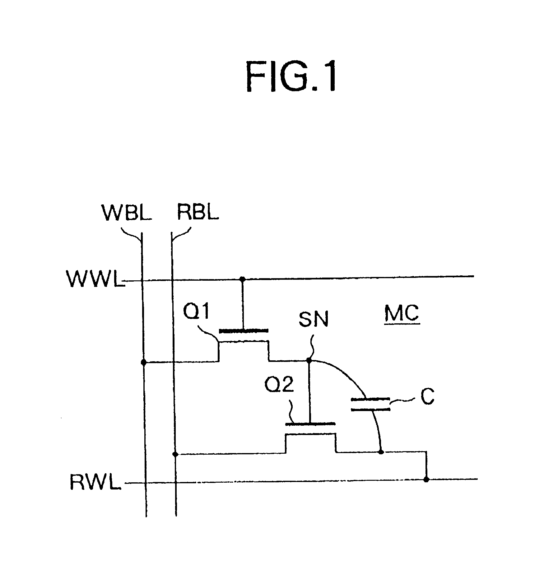
In the first embodiment, the fundamental configuration and the operation principle of a memory cell according to the present invention will be schematically explained. Note that, in the present embodiment, the case where two bit lines are provided for a write operation and read operation is taken as the example, but it is also possible to commonly use one bit line.
FIG. 1 is a circuit diagram of a memory cell according to the first embodiment.
A memory cell MC shown in FIG. 1 is configured by a write transistor Q1, read transistor Q2, and capacitor C. In the write transistor Q1, the gate is connected to the write word line WWL, and one of the source or drain is connected to the write bit line WBL. In the read transistor Q2, the gate is connected to the other of the source or drain of the write transistor Q1, the source is connected to the read bit line RBL, and the drain is connected to the read word line RWL. One electrode of the capacitor C is connected to a middle point of connecti...
second embodiment
In the second embodiment, a more detailed explanation will be made by using a concrete example of the configuration of the memory cell array and its peripheral circuits and the plane and sectional structure of the memory cell.
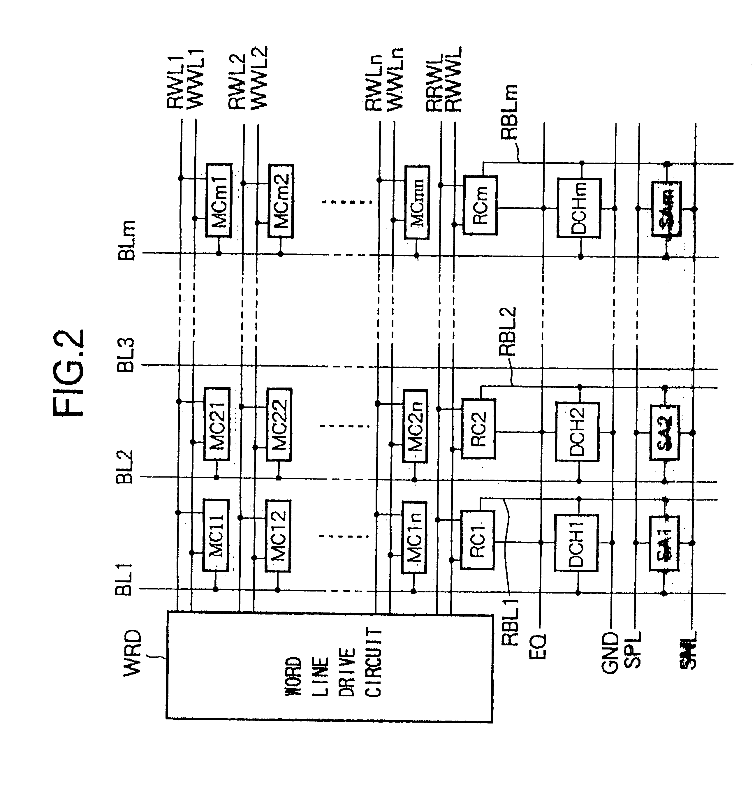
FIG. 2 is a block diagram of principal parts of the memory cell array and peripheral circuits including a word line drive circuit, sense amplifiers, and discharge circuits in the semiconductor memory according to the second embodiment.
As illustrated, the memory cell array is configured by m.times.n (m, n: any natural numbers) number of memory cells MC11, MC12, . . . MC21, . . . , and MCmn arranged in a matrix. In the memory cell array, the memory cells of the same row are connected to the same write word lines WWLj (j=1, 2, . . . , n) and read word lines RWLj, and the memory cells of the same column are connected to the same bit line BLi (i=1, 2, . . . , m). A reference cell (reference memory cell) RCi, a sense amplifier SAi, and a discharge circuit DCHi are co...
third embodiment
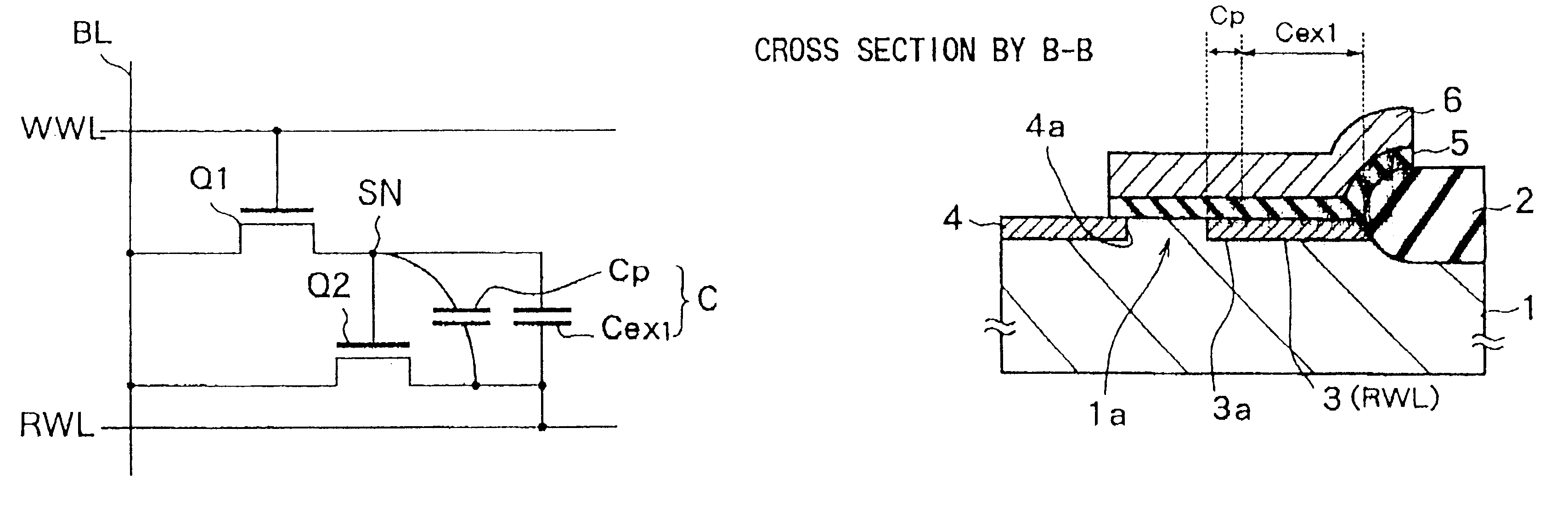
The third embodiment relates to a modification of the memory cell capable of increasing the capacitance between the gate and the drain of the read transistor while preventing the increase of the area of the memory cell as much as possible.
FIG. 12 is a circuit diagram of a memory cell according to the third embodiment.
The difference of this memory cell from the second embodiment resides in that an external capacitance element Cex1 is connected in parallel to the transistor parasitic capacitance Cp. The rest of the configuration is similar to that of the memory cell according to the second embodiment shown in FIG. 4.
FIGS. 13A and 13B are a plan view and sectional view of the connection portion of the read transistor in which the capacitor is formed and the read word line in the memory cell according to the third embodiment.
Compared with the case of the second embodiment shown in FIGS. 5A and 5B, in this memory cell, the gate electrode 6 is extended up to the element isolation insulati...
PUM
 Abstract
Description
Claims
Application Information
 - Generate Ideas
- Intellectual Property
- Life Sciences
- Materials
- Tech Scout
- Unparalleled Data Quality
- Higher Quality Content
- 60% Fewer Hallucinations
Browse by: Latest US Patents, China's latest patents, Technical Efficacy Thesaurus, Application Domain, Technology Topic, Popular Technical Reports.
© 2025 PatSnap. All rights reserved.Legal|Privacy policy|Modern Slavery Act Transparency Statement|Sitemap|About US| Contact US: help@patsnap.com