Semiconductor device and method of fabricating the same

a technology of semiconductor devices and semiconductor materials, applied in semiconductor devices, semiconductor/solid-state device details, electrical apparatus, etc., can solve problems such as short circuits, difficult to embed wiring materials into through-holes, and high temperatur

Inactive Publication Date: 2001-12-04
SEIKO EPSON CORP
View PDF14 Cites 48 Cited by
  • Summary
  • Abstract
  • Description
  • Claims
  • Application Information

AI Technical Summary

Benefits of technology

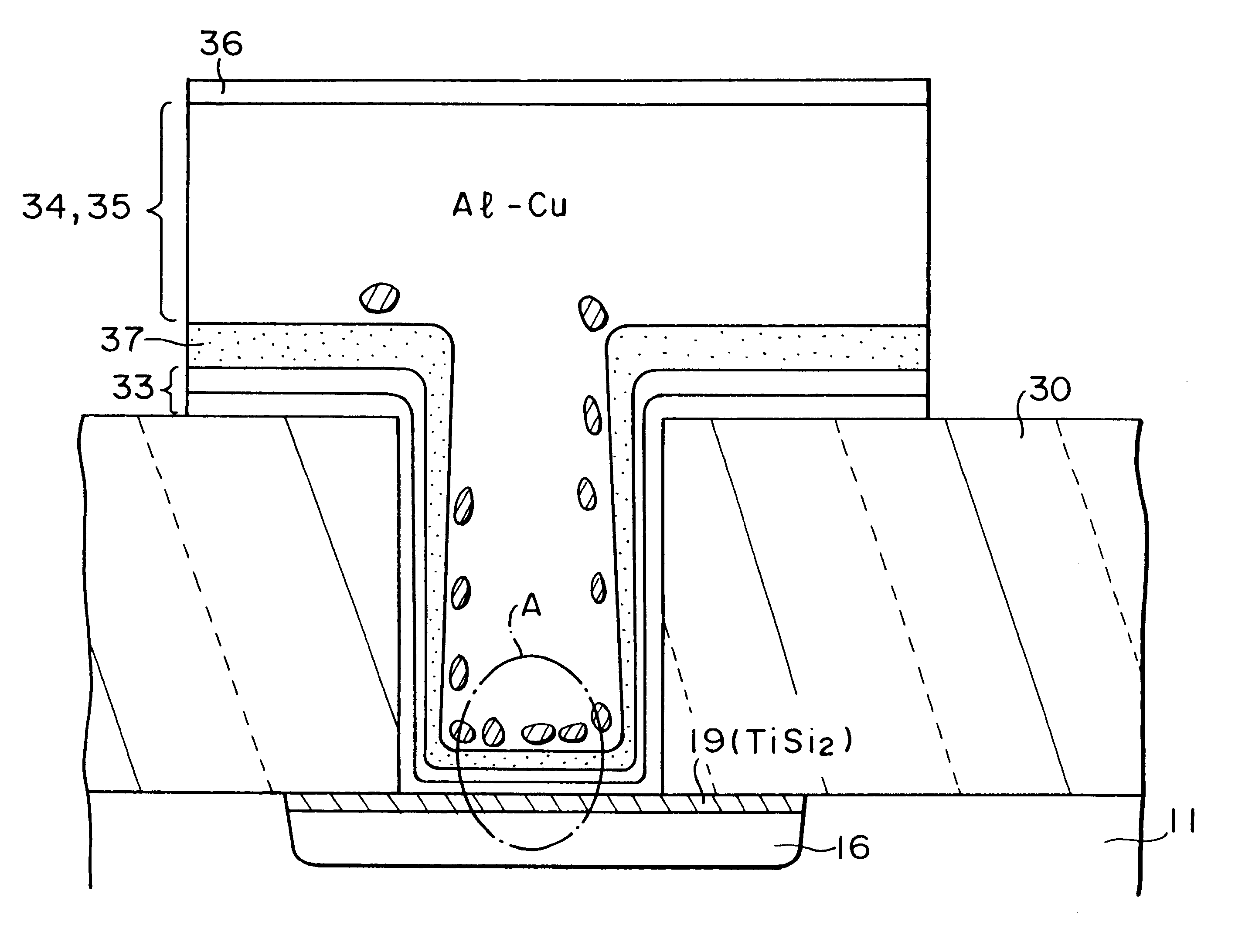
Beryllium is also capable of occluding oxygen. For instance, beryllium occludes oxygen which is produced from silicon oxide of an interlayer dielectric and exists in an aluminum alloy to improve the fluidity of aluminum and the capability of embedding an aluminum alloy in a through-hole.
The inventors of the present invention have confirmed that gas produced from such an interlayer dielectric is absorbed by an intermediate layer such as a barrier layer or a wetting layer but is not absorbed by an aluminum layer formed in the through-hole. It is therefore possible to positively restrain a reduction in the wettability of the intermediate layer and the occurrence of voids, caused by the presence of such a gas between the intermediate layer and the first aluminum layer, by eliminating the gasifiable components contained in the interlayer dielectric. This results in the formation of a contact portion comprising an aluminum layer with high coverage and low resistance in the through-hole.

Problems solved by technology

It is difficult to embed wiring materials into such through-holes, and this has become an important technical problem in recent years.
Customary methods, however, require high temperature in sputtering to bury aluminum or an aluminum alloy in a through-hole.
As the temperature increases, whiskers are easily produced, causing short circuits between wires, and aluminum of a wiring layer in the through-hole reacts with silicon in a substrate giving easy rise to electrical characteristic problems such as leaks.
However, if the wiring layer is thin, the electro-migration resistance is reduced and hence conventionally used aluminum alloy materials cannot adequately cope with this phenomenon.
This results in resistance to a rise in the electric characteristics problem such as leaks.
This results in the formation of a contact portion comprising an aluminum layer with high coverage and low resistance in the through-hole.

Method used


Image

  • Semiconductor device and method of fabricating the same
  • Semiconductor device and method of fabricating the same
  • Semiconductor device and method of fabricating the same

Examples


experimental example

(1) Electro-migration Resistance of a Metal Wiring Layer

The ratio (wt %) of beryllium to copper which were added to an aluminum alloy was altered to measure the defect ratio in an electro-migration test. The results are shown in FIG. 8. In FIG. 8, the stress time, namely the time during which current flows, is plotted along the horizontal axis, and the defect ratio is plotted along the vertical axis. Also, "a", "b", "c" and "d" in FIG. 8 show the results when the following metals were added to aluminum respectively.

"a": copper (0.5 wt %)

"b": copper (0.5 wt %), beryllium (0.1 wt %)

"c": copper (0.5 wt %), beryllium (0.3 wt %)

"d": copper (0.1 wt %), beryllium (0.3 wt %)

It is confirmed from FIG. 8 that, compared with the case of adding only copper to aluminum, a further addition of beryllium to aluminum containing copper reduces the defect ratio. It is also seen from the data shown by the symbols a and b in the graph that the defect ratio decreases as the amount of beryllium increases. ...


PUM

PropertyMeasurementUnit
temperatureaaaaaaaaaa

Abstract

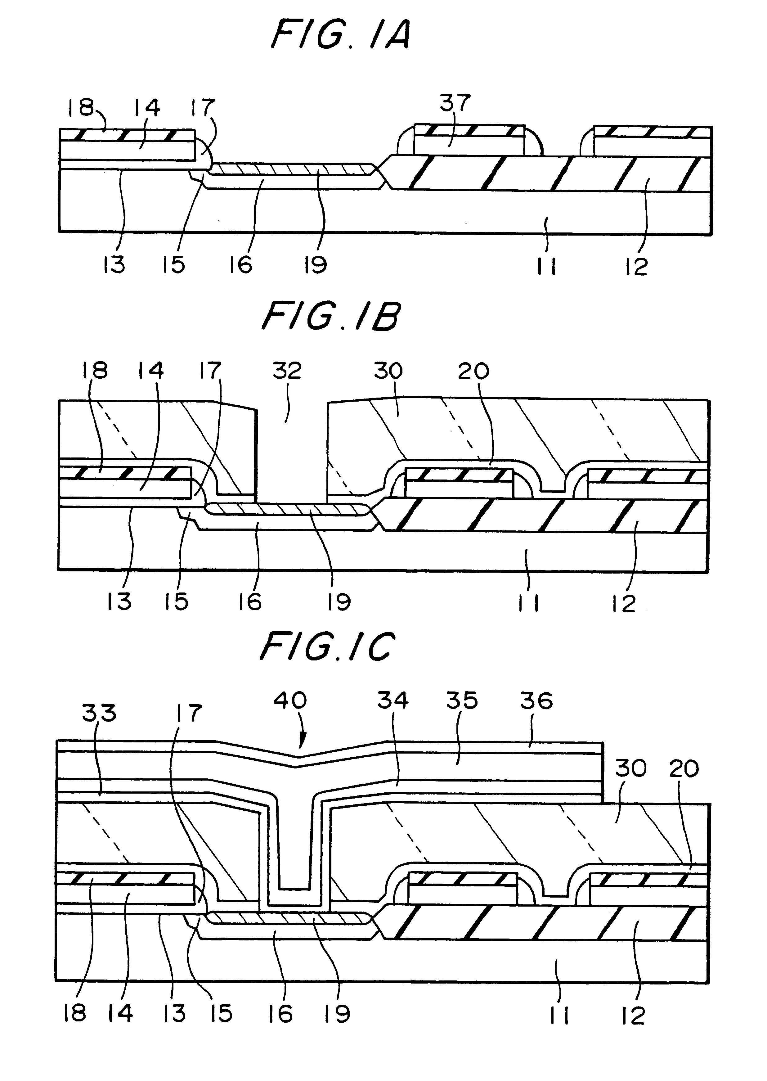
A semiconductor device comprising a semiconductor substrate including an electronic element such as a MOSFET, interlayer dielectric (silicon oxide layer or BPSG layer) formed on the semiconductor substrate, a through-hole formed in the interlayer dielectric, a barrier layer formed on a surface of the interlayer dielectric and on a surface of the through-hole, and a metal wiring layer formed on the barrier layer. The metal wiring layer contains aluminum as its major component and 0.1 wt % to 3 wt % of beryllium. An aluminum alloy can be embedded in the through-hole without creation of any void or breaking of wire, and the semiconductor device is highly resistant to electro-migration.

Description

1. Field of the InventionThe present invention relates to a semiconductor device and a method of fabricating the same, and, more particularly, to a semiconductor device which can be miniaturized and has a wiring layer made of an aluminum alloy having high electro-migration resistance, and to a method of fabricating the same.2. Description of Related ArtIn semiconductor devices such as LSIs, recent advances in miniaturization, integration, and multi-layering of electronic elements have required through-holes with a large aspect ratio. It is difficult to embed wiring materials into such through-holes, and this has become an important technical problem in recent years. Therefore, attempts have been made to embed aluminum or an aluminum alloy which is useful as a wiring material into the through-holes.Customary methods, however, require high temperature in sputtering to bury aluminum or an aluminum alloy in a through-hole. As the temperature increases, whiskers are easily produced, caus...

Claims


Application Information

Patent Timeline
Patent Type & Authority Patents(United States)
IPC IPC(8): H01L23/532H01L21/70H01L23/485H01L21/285H01L23/52H01L21/768H01L21/02H01L21/3205H01L23/48H01L21/316H01L21/28H01L21/283
CPCH01L21/28518H01L21/2855H01L21/32051H01L21/76801H01L21/76802H01L21/76828H01L21/76843H01L21/76846H01L21/76856H01L21/76877H01L23/485H01L23/53223H01L21/31612H01L21/31625H01L2924/0002H01L2924/00H01L21/02129H01L21/02164H01L21/283
Inventor ASAHINA, MICHIOMATSUMOTO, KAZUKISUZUKI, EIJI
Owner SEIKO EPSON CORP
Why Eureka
Try Eureka