

E-beam shape aperature incorporating lithographically defined heater element
a heater element and electron beam technology, applied in photomechanical equipment, instruments, nuclear engineering, etc., can solve the problems of reducing useful production time, severely compromising manufacturing efficiency, and unavoidable contamination in electron beam systems
- Summary
- Abstract
- Description
- Claims
- Application Information
AI Technical Summary
Problems solved by technology
Method used
Image

Examples
Embodiment Construction
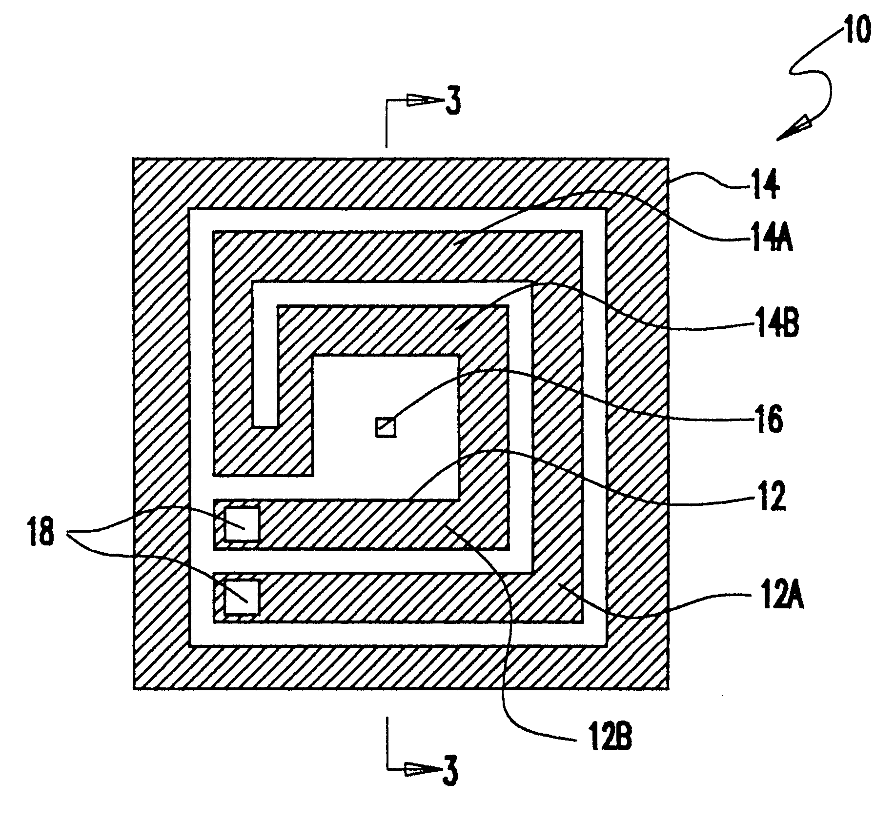
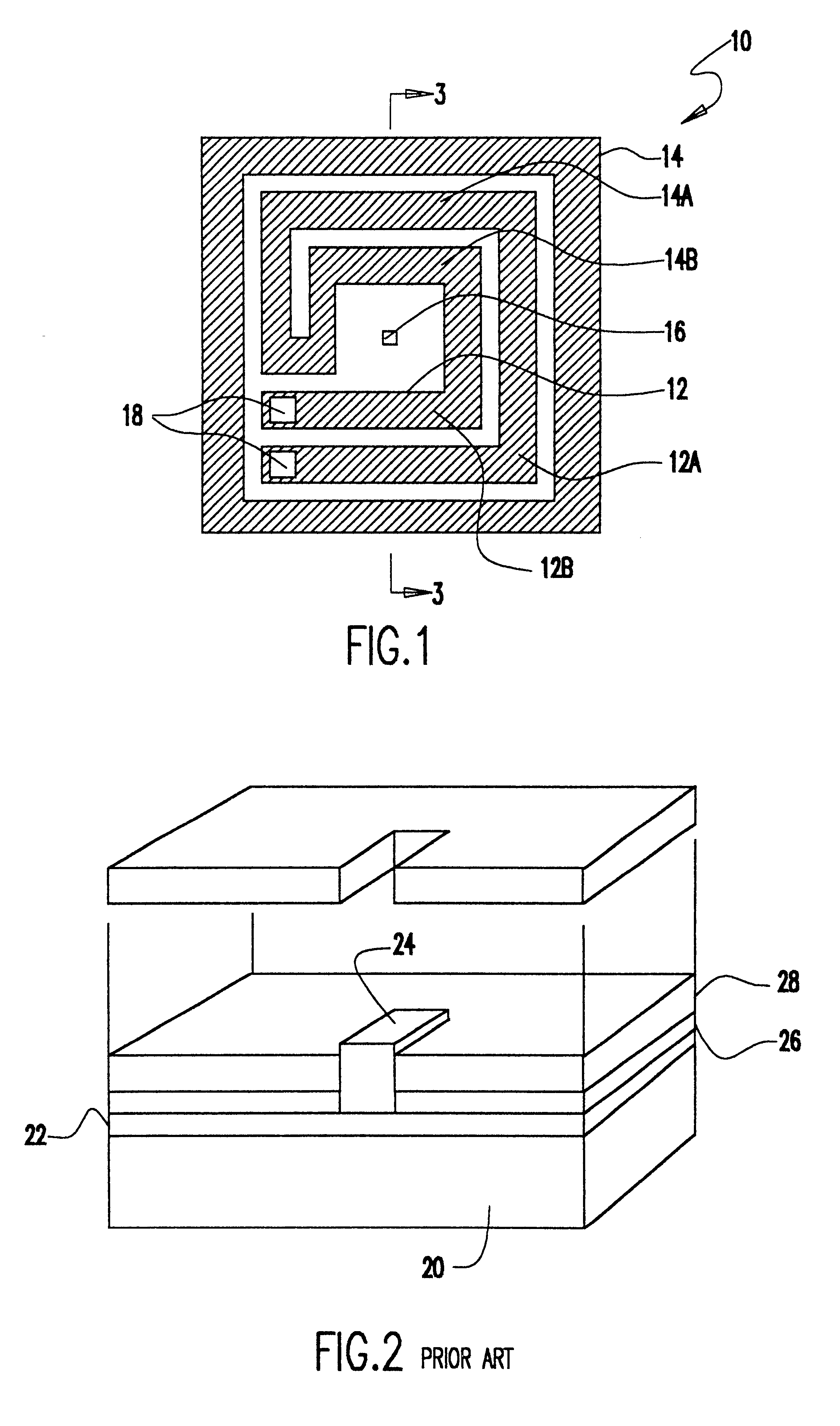
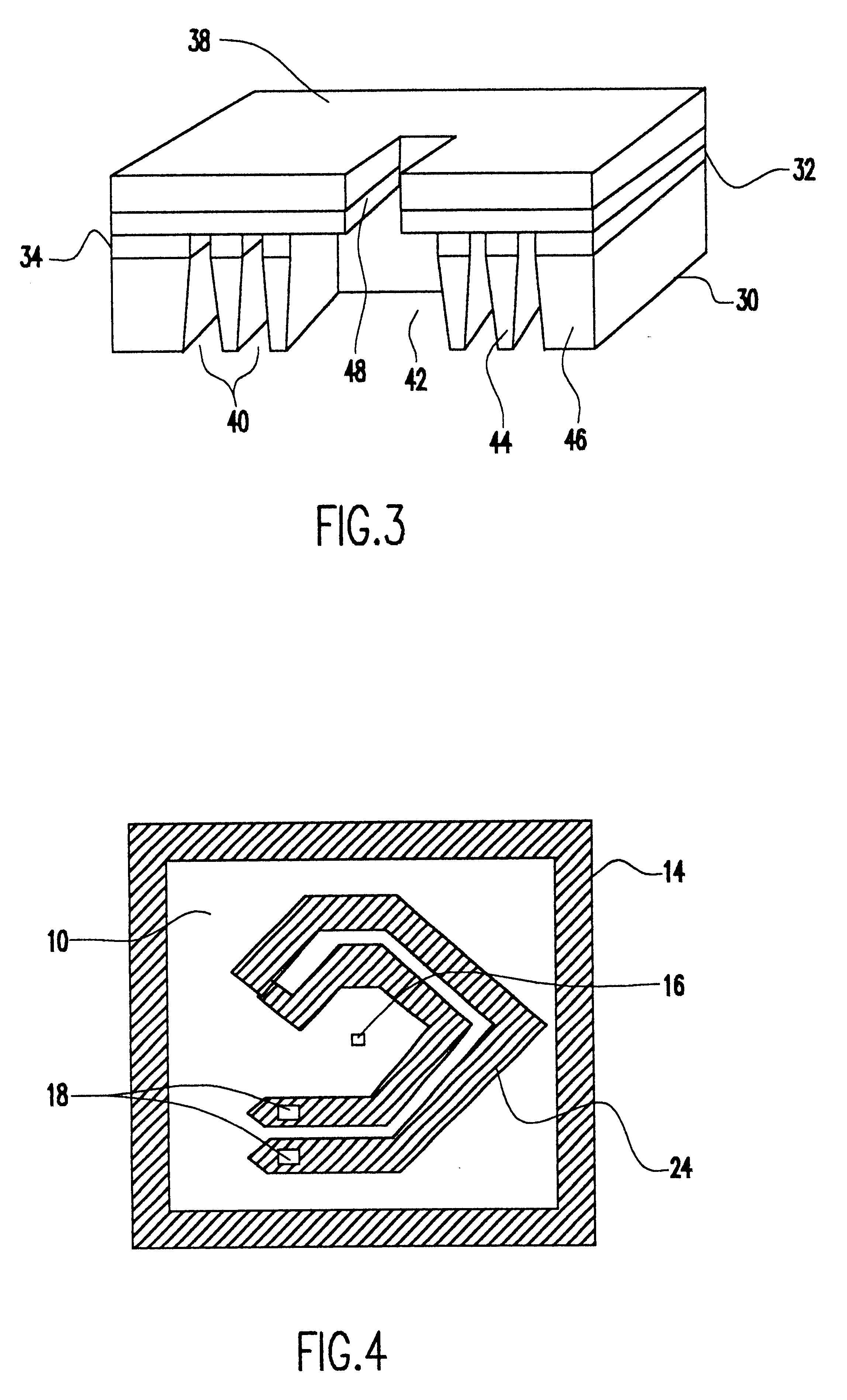
Referring now to the drawings, and more particularly to FIG. 1, there is shown, in plan view, a surface of an aperture plate 10 including a preferred pattern of a serpentine heater element 12. When the aperture plate 10 is installed in an electron beam lithographic tool, as is preferred, the surface shown will generally face away from the charged particle or electron source. Since electron beam lithographic tools are generally arranged with a vertical beam column with the source at the top, the surface shown in FIG. 1 will generally face downwardly and thus will sometimes be referred to hereinafter as the back or bottom surface of aperture plate 10. Similarly, the opposite side of the aperture plate 10 will sometimes be referred to hereinafter as the front or top surface.
Heater element 12 preferably substantially surrounds the aperture 16 at a distance therefrom corresponding to about ten times the transverse dimension of the aperture or beam and is preferably serpentine shaped to p...
PUM
 Abstract
Description
Claims
Application Information