
Super-wide band shielding materials

a shielding material and super-wide band technology, applied in the direction of natural mineral layered products, nuclear engineering, nuclear elements, etc., can solve the problems of relatively little information regarding microwave absorption for stealth technology, and the inability of polymers to perform alone in an acceptable frequency rang

Inactive Publication Date: 2002-04-30
FRACTAL SYST INC
View PDF9 Cites 26 Cited by
  • Summary
  • Abstract
  • Description
  • Claims
  • Application Information

AI Technical Summary

Benefits of technology

It is another object of the invention to provide improved shielding materials having low weight and low cost.
It is a further object of this invention to provide improved shielding materials having applicability over a wide frequency range, and which can be tailored to a specific application.

Problems solved by technology

However, all of the above work, apart from the camouflaging textiles and shielded cables, use synthesized polymers with no variation in characteristics or parameters for their intended applications.
These polymers cannot perform alone in an acceptable frequency range.
Other than EMI shielding, which needs high conductivity, relatively little information was available concerning microwave absorption for stealth technology.

Method used

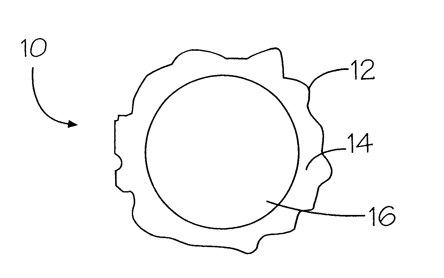
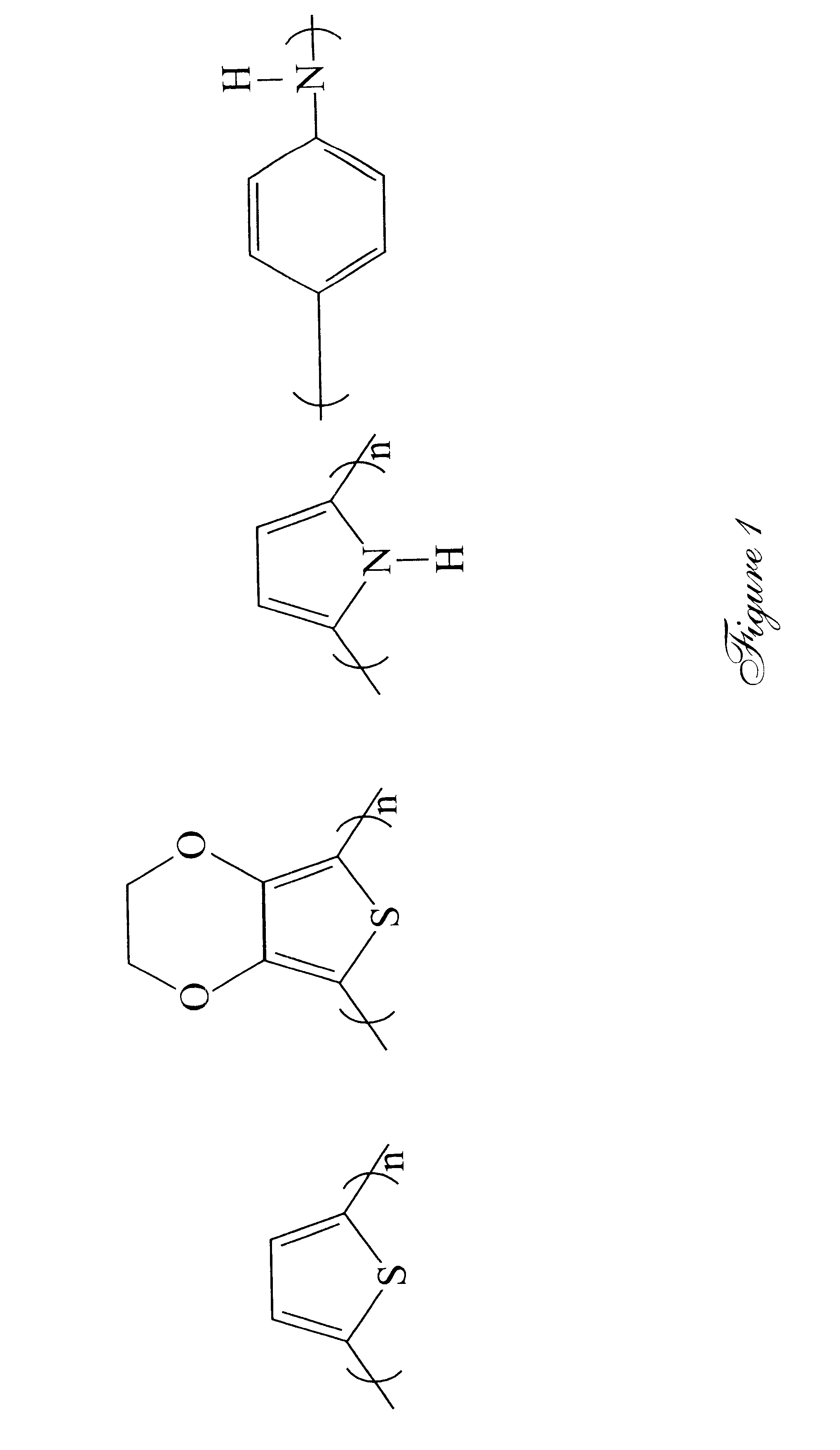
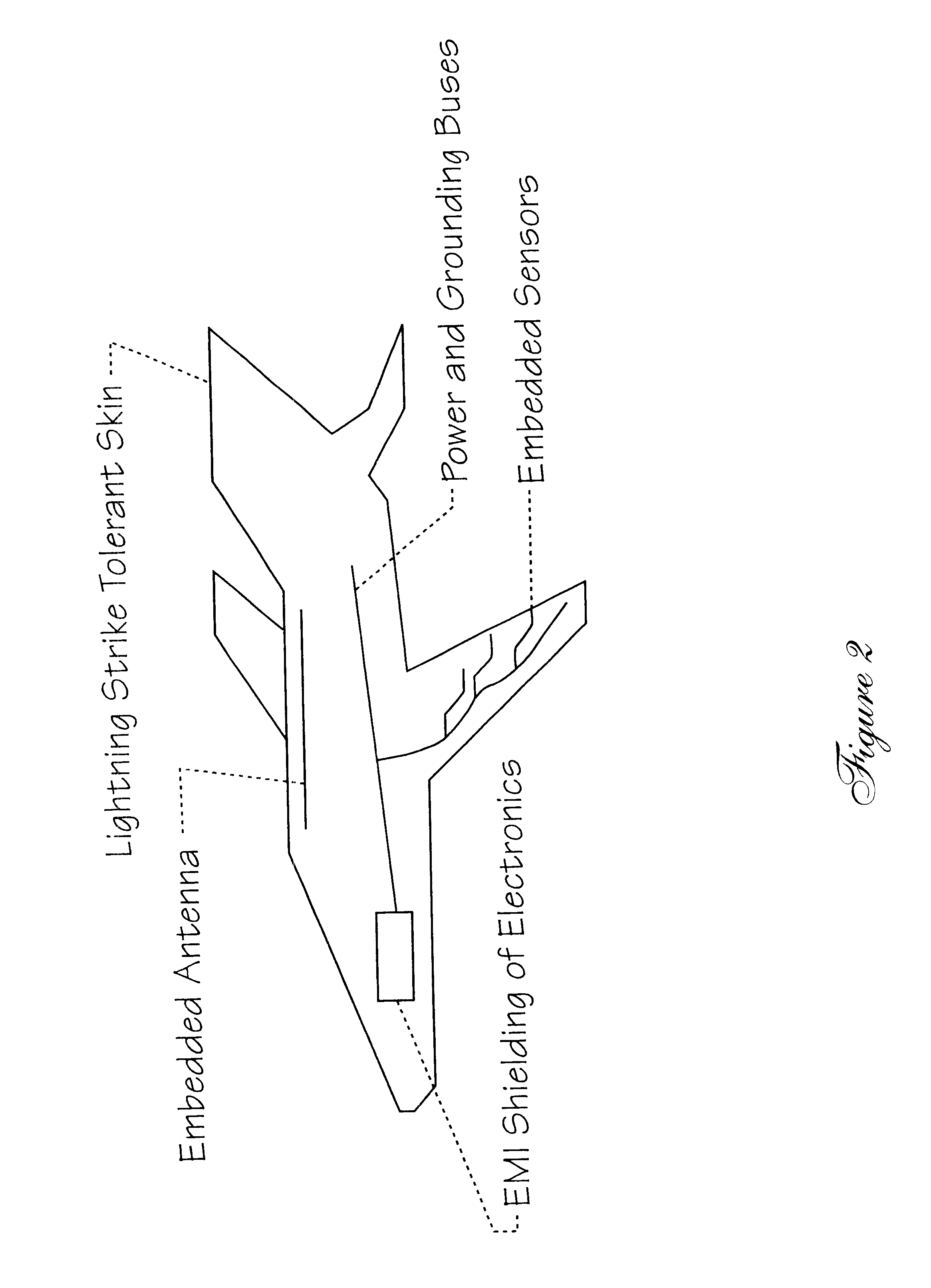

Image

  • Super-wide band shielding materials
  • Super-wide band shielding materials
  • Super-wide band shielding materials

Examples


example ii

The nickel and conductive polymer layers of the shielding material of Example I is formed using electroless plating and oxidative polymerization, respectively.

example iii

The same material as Example I is formed, with the exception that the nickel layer is 3 weight percent, and 50 nanometers thick.

example iv

The same material as Example III, except that the conductive polymer layer is two weight percent, and has a thickness of 1 .mu.m. Bulk conductivity is 150 S / cm, and shielding effectiveness is 82 dB at 1 GHz.

References

1. A. J. Epstein et al. in "Intrinsically Conduction Polymers: an Emerging Technology", Ed. M. Aldissi, p. 165 (1993), Kluwer Academic Publishers, Dordrecht, The Netherlands.

2. L. W. Shacklette and N. F. Colaneri, IEEE Instrumentation and Measurement Technology Conf., Atlanta, Ga., May 14-16, 1991.

3. M. Aldissi, "Metal-Coated Shielding Materials and Articles Fabricated Therefrom", U.S. Pat. No. 5,171,937.

4. M. Aldissi, "Shielded Wire and Cable", U.S. Pat. No. 5,180,884.

5. M. Aldissi, "Conductive Polymeric Shielding Materials Using Shaped Ferrites", U.S. Pat. No. 5,206,459.

6. M. Aldissi, "Polymeric Electromagnetic Fluids", U.S. patent application Ser. No. 07 / 933,554 now abandoned.

7. M. Aldissi, "Electromagnetic Bonding Materials", U.S. patent application Ser. No. 07 / 968,...


PUM

PropertyMeasurementUnit
Fractionaaaaaaaaaa
Fractionaaaaaaaaaa
Fractionaaaaaaaaaa

Abstract

Shielding materials are fabricated from a new three-layered particle having a core, a metal layer, and a conductive polymer layer. The new particles are blended into a polymer matrix and processed in the absence or under the influence of a magnetic field to form single-layered coatings and freestanding films and sheets. The magnetically processed materials yield a conductive network of particles rather than discrete particles randomly disposed within the polymeric medium.

Description

The present invention relates to shielding materials and, more particularly, to a new, multi-layered particle of metal coated ferrites coated with a conductive polymer, and networked into a conductive polymer matrix to produce single-layered shielding coatings, films and sheets having a tailored application in sophisticated electronics and military hardware.Sophisticated electronics, particularly those employing high frequencies and military hardware using space-age composites, require electromagnetic radiation hardening. Survivability countermeasures use shielding against nuclear, laser, EMI and radar / microwave radiation. Several hardening methods exist. The choice of which techniques to use depends on the frequency range and the type of the electromagnetic threat. Surface metallization, use of conductive composites, and metallic enclosures, are but a few of the shielding techniques employed. Each method has its own shortcomings, and the materials used are often expensive.It is not...

Claims


Application Information

Patent Timeline
IPC IPC(8): B22F1/02G21F1/00G21F1/10H01B1/22B22F1/17B22F1/18
CPCB22F1/025G21F1/10H01B1/22G21Y2002/301G21Y2002/302Y10T428/2933G21Y2004/30G21Y2004/40Y10T428/2991G21Y2002/304B22F1/17B22F1/18
Inventor ALDISSI, MAHMOUD
Owner FRACTAL SYST INC
Learn More