Triple metal line 1T/1C ferroelectric memory device and method for fabrication thereof

a ferroelectric memory and metal line technology, applied in semiconductor devices, electrical devices, capacitors, etc., can solve the problems of difficult data delivery, oxidation at the interface between the lower electrode and the contact plug, and inability to produce reliable electrical ohmic conta

Inactive Publication Date: 2002-05-14
SAMSUNG ELECTRONICS CO LTD
View PDF9 Cites 53 Cited by
  • Summary
  • Abstract
  • Description
  • Claims
  • Application Information

AI Technical Summary

Problems solved by technology

The aforementioned high temperature annealing processes cause oxidation at the interface between the lower electrode and the contact plug.
Such oxidation at the interfaces cannot produce a reliabl

Method used


Image

  • Triple metal line 1T/1C ferroelectric memory device and method for fabrication thereof
  • Triple metal line 1T/1C ferroelectric memory device and method for fabrication thereof
  • Triple metal line 1T/1C ferroelectric memory device and method for fabrication thereof

Examples


Embodiment Construction

Applicants' Korean Patent Application No. 99-30398, filed Jul. 26, 1999, is incorporated herein by reference as if fully set forth herein.

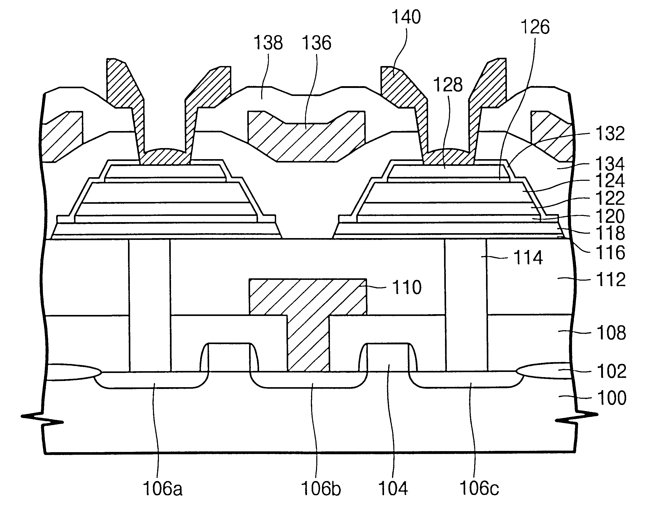
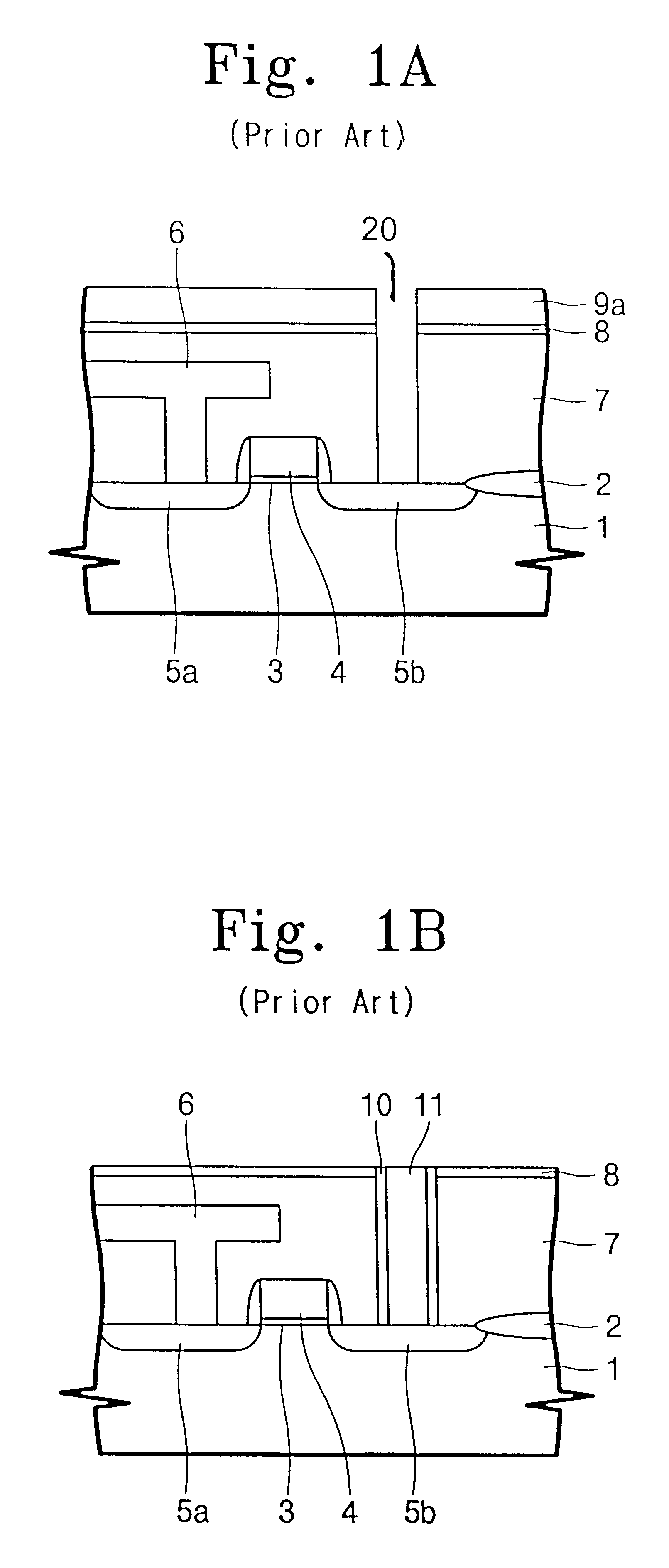
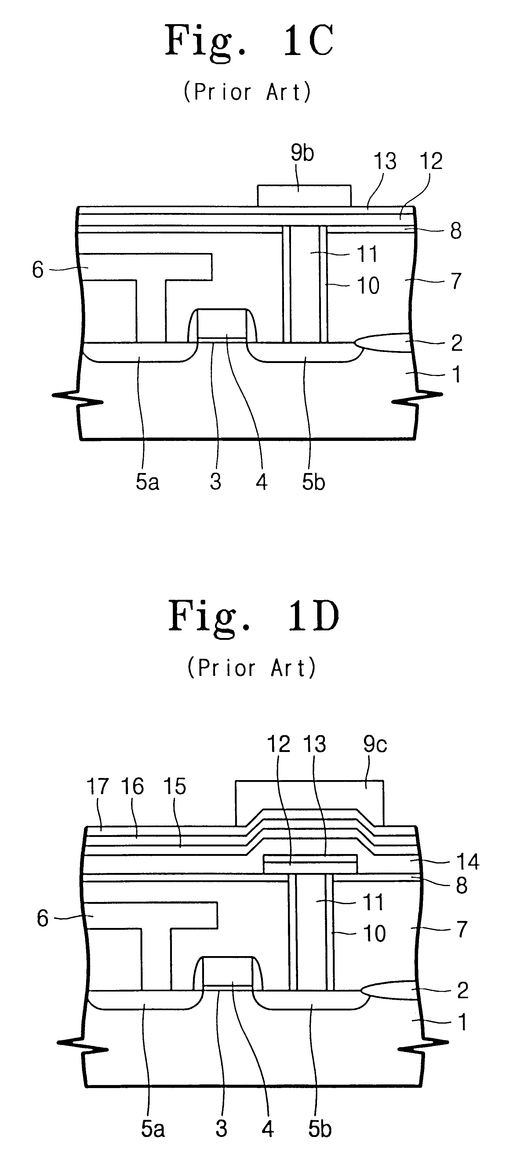
The formation of the FRAM cell includes certain process steps that are well known in the art. For example, the processes of photolithography, masking, and etching are used extensively in several embodiments of the present invention. One standard photolithographic process includes creating a photolithographic mask containing the pattern of the component to be formed; coating the wafer with a light sensitive material, such as a photoresist; exposing the photoresist-coated wafer to ultra-violet light through the mask to soften or harden various parts of the photoresist (depending on whether a positive or negative photoresist is used); removing the materials left unprotected by the photoresist; and then stripping the remaining photoresist. Another well-known process that is used extensively in this and many other integrated circuit fabrication process...


PUM


Abstract

Disclosed is a triple metal line 1T/1C ferroelectric memory device and a method to make the same. A ferroelectric capacitor is connected to the transistor through a buried contact plug. An oxidation barrier layer lies between the contact plug and the lower electrode of the capacitor. A diffusion barrier layer covers the ferroelectric capacitor to prevent diffusion of material into or out of capacitor. As a result of forming the oxidation barrier layer, the contact plug is not exposed to the ambient oxygen atmosphere thereby providing a reliable ohmic contact between the contact plug and the lower electrode. Also, the memory device provides a triple interconnection structure made of metal, which improves device operation characteristics.

Description

1. Field of the InventionThe present invention relates to a ferroelectric memory device, and more particularly to a triple metal line, one transistor and one capacitor (1T / 1C) ferroelectric memory device and a method for fabrication thereof.2. Background of the InventionModern data processing systems require that a substantial portion of the information stored in their memory be randomly accessible to ensure rapid access to such information. Ferroelectric random access memories (FRAMs) have been proposed because of their high-speed operational speeds. FRAMs also exhibit a significant advantage of being non-volatile. This is achieved by the fact that a ferroelectric capacitor includes a pair of capacitor electrodes having ferroelectric material placed in between. FRAMs have two different, stable polarization states, which can be defined with a hysteresis loop by plotting polarization against applied voltage. Ferroelectric memory elements are programmable with less than 5V (flash memo...

Claims


Application Information

Patent Timeline
IPC IPC(8): H01L21/70H01L27/115H01L21/8246H01L21/02H01L21/316H01L27/105H01L27/10
CPCH01L27/11507H01L27/11502H01L21/31604H01L21/3162H01L28/75H01L28/55H10B53/30H10B53/00H01L21/02178H01L21/02263H01L27/10
Inventor JUNG, DONG-JINKIM, KI-NAM
Owner SAMSUNG ELECTRONICS CO LTD
Why Eureka
Try Eureka