Method and apparatus for chip placement

a technology of electronic chips and placement methods, applied in metal working apparatuses, metal-working machine components, manufacturing tools, etc., can solve the problems of increasing the cost of such devices to prohibitive levels and degrading the operating speed

Inactive Publication Date: 2002-05-21
MICRO ROBOTICS SYST
View PDF25 Cites 52 Cited by
  • Summary
  • Abstract
  • Description
  • Claims
  • Application Information

AI Technical Summary

Benefits of technology

Another object of this invention is to provide a method and apparatus for precisely locating electrical terminals on a supporting structure with bonding pads on an electronic chip.
Still another object of this invention is to provide a method and apparatus for enhancing the capability of conventional assembly apparatus to perform precise positioning of an electronic chip on a supporting structure in an automated manufacturing apparatus with an insignificant impact on production rates.
In accordance with another aspect of this invention, first and second supports positioning first and second components, each having alignment features, maintain the second component at a reference plane while the first support locates the first component proximally to the second component on one side of the reference plane. An image generator having a given depth of field characteristic images the alignment features from the other side of the reference plane when the alignment features are within the depth of field of the image generator. An optical path directs an enlarged image to a location where portions of the enlarged image are converted into electronic video signals that enable the first and second component to be brought into contact in precise registration.

Problems solved by technology

Moreover, at this requirement for precision changes in temperature require elaborate and time-consuming calibration procedures that further degrade operating speed.
The alternative of increasing the inherent accuracy of the robotic devices will increase the costs of such devices to prohibitive levels.

Method used


Image

  • Method and apparatus for chip placement
  • Method and apparatus for chip placement
  • Method and apparatus for chip placement

Examples


Embodiment Construction

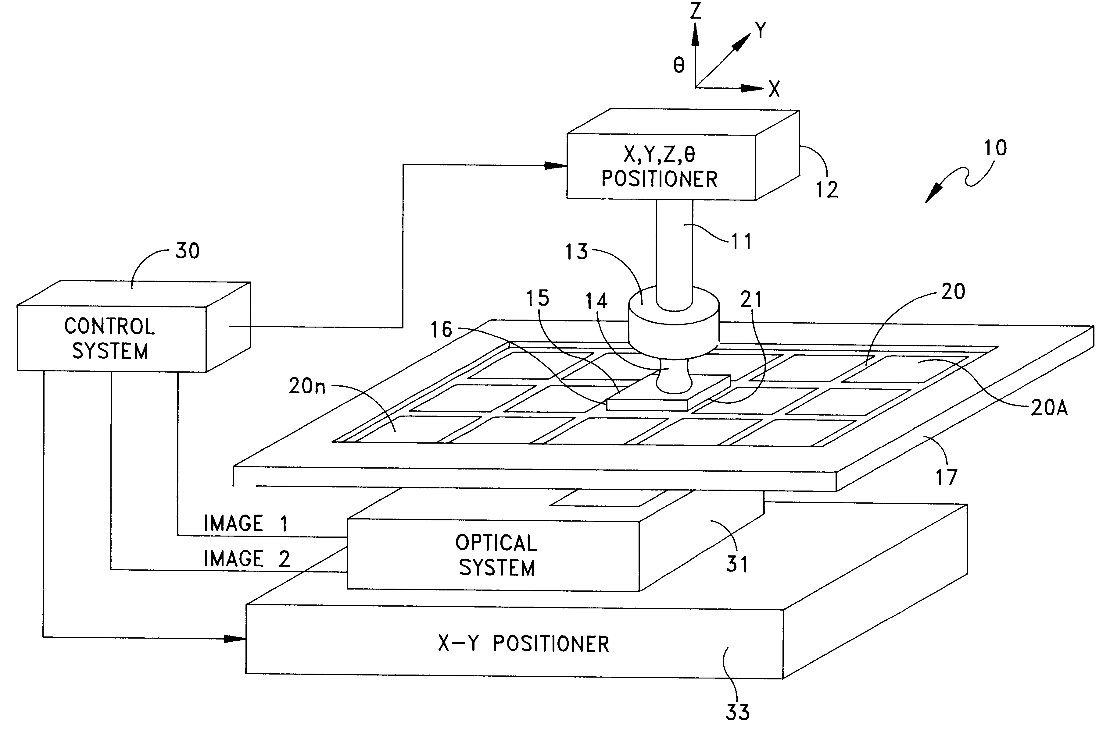
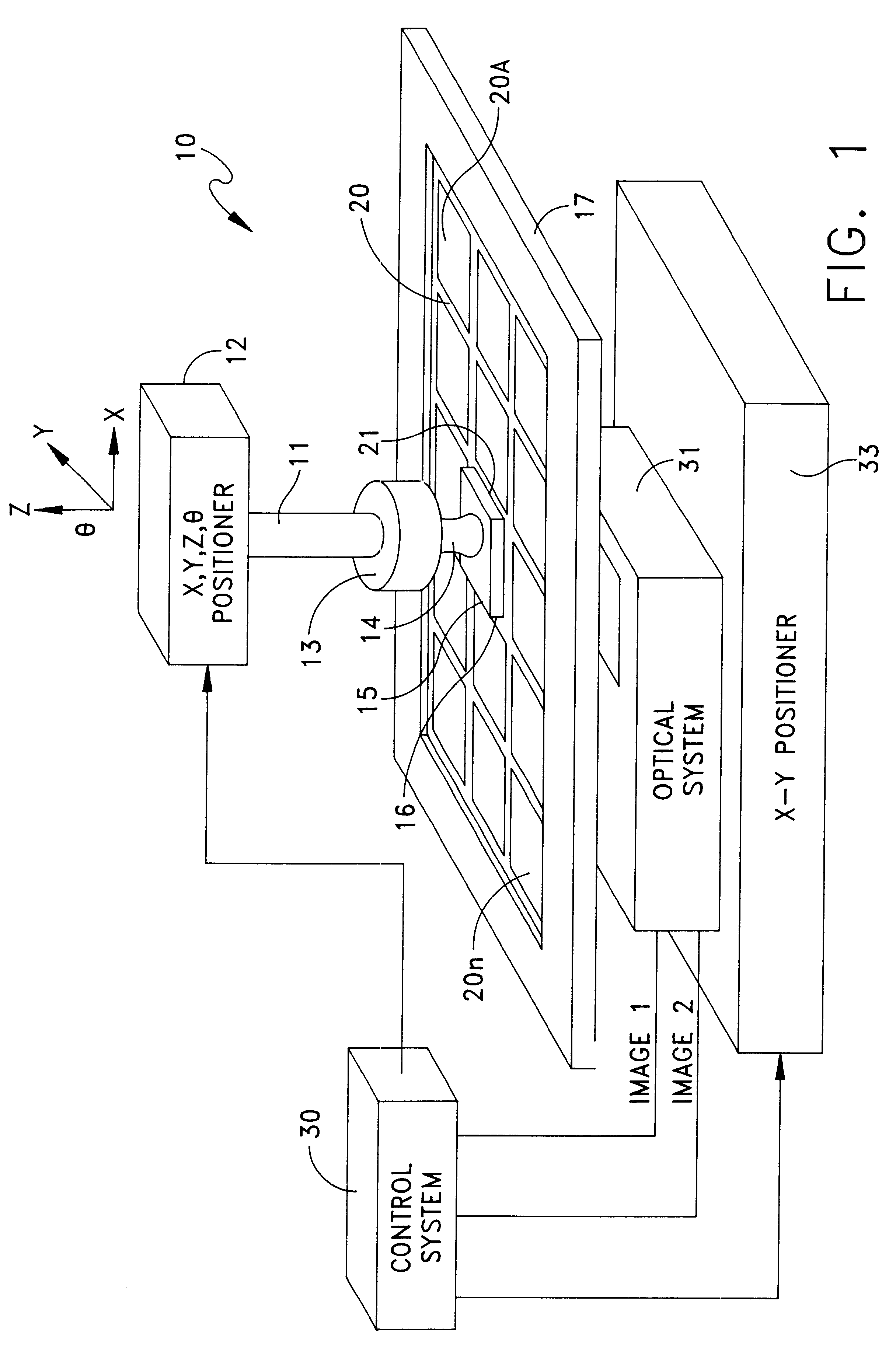
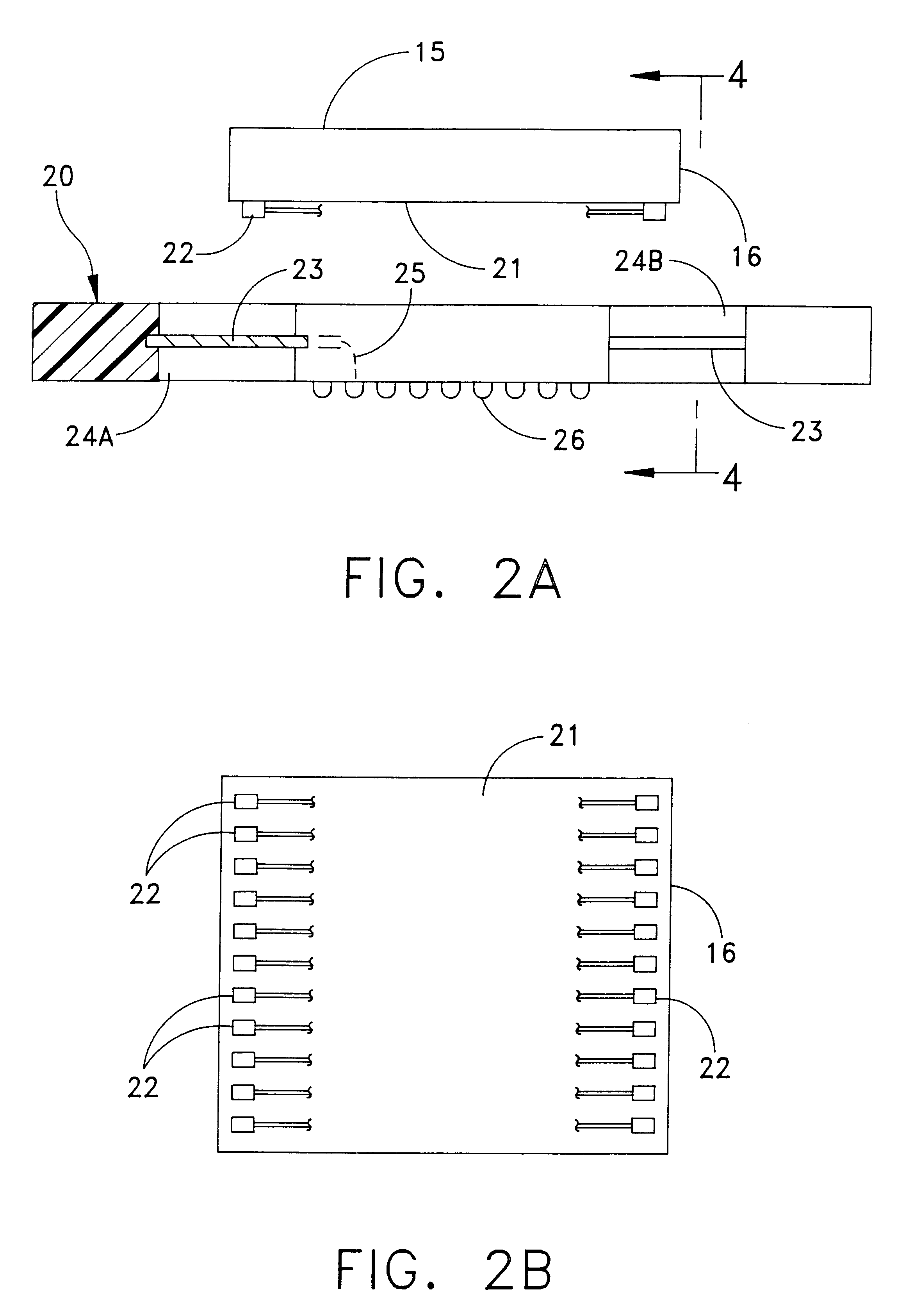
FIG. 1 schematically depicts a robotic system 10 adapted for implementing this invention. The robotic system 10 includes a robotic arm 11 and a positioner 12 capable of moving the arm 11 in a horizontal x-y plane, and along a vertical, or z axis that is perpendicular to the x-y plane. In addition a chuck 13 at the end of the arm 11 is generally adapted for rotating about the z axis for angular, or .THETA., motion. Conventionally the chuck 13 carries a vacuum gripper 14 that contacts an upper surface 15 of an electronic chip 16, as first component, thereby to carry and support the electronic chip or component. The positioner 12 therefore is able to locate the electronic chip 16 in any of "x", "y", "z" and ".THETA." degrees of freedom. A substrate support 17, typically a fixture mounted in the robotic system 10, carries a substrate in the form of a tape 20 as a second component having a plurality of leads.

Such robotic systems are well known in the art. Consequently detailed discussion...


PUM

PropertyMeasurementUnit
widthaaaaaaaaaa
widthaaaaaaaaaa
distanceaaaaaaaaaa

Abstract

A method and apparatus for accurately registering electronic chip bonding pads with substrate leads. Images are developed of different portions of the interface between the electronic chip and the substrate by reflecting collimated, parallel light from the bottom of the chip through transparent areas of the substrate. Image analysis of the composite, superimposed images from spaced positions containing the bonding pads and the leads provide a corrective positioning after which the electronic chip and substrate are brought into contact.

Description

1. Field of the InventionThis invention is generally directed to a method and apparatus for bringing a component into register with a support with a high degree of precision. More particularly this invention relates to the precise alignment of an electronic chip on a supporting structure.2. Description of Related ArtConsiderable effort has been directed to developing methods and apparatus for precisely positioning one component, such as an electronic chip, on a second component, such as a supporting structure or substrate of any of diverse forms. In accordance with one prior art approach, a robotic device includes a video system to bring bonding pads on a semiconductor device, as the one component or piece, into registration with leads on a substrate as a supporting structure as a second component or piece. Basically, the video system images features on each of the component and supporting structure when they are at locations remote from a work station at which they will actually be...

Claims


Application Information

Patent Timeline
Patent Type & Authority Patents(United States)
IPC IPC(8): H01L21/68H01L21/67H05K13/04
CPCH01L21/681H05K13/0413Y10T29/53178Y10T29/53087Y10T29/49131H05K13/0812H05K3/32
Inventor SRIVASTAVA, NILENDUDEVASIA, CYRIACSUN, SUNG PING
Owner MICRO ROBOTICS SYST
Why Eureka
Try Eureka