PE-silane oxide particle performance improvement

a technology of silane oxide and performance improvement, applied in the field of pesilane oxide particle performance improvement, can solve problems such as particle spiking disaster

Inactive Publication Date: 2002-06-04
TAIWAN SEMICON MFG CO LTD
View PDF1 Cites 37 Cited by
  • Summary
  • Abstract
  • Description
  • Claims
  • Application Information

AI Technical Summary

Problems solved by technology

Abnormal nucleation sites are formed by the SiH.sub.4 on the wafer surface resulting in the particle spiking disaster observed by the inventors.

Method used


Image

  • PE-silane oxide particle performance improvement
  • PE-silane oxide particle performance improvement
  • PE-silane oxide particle performance improvement

Examples


second embodiment

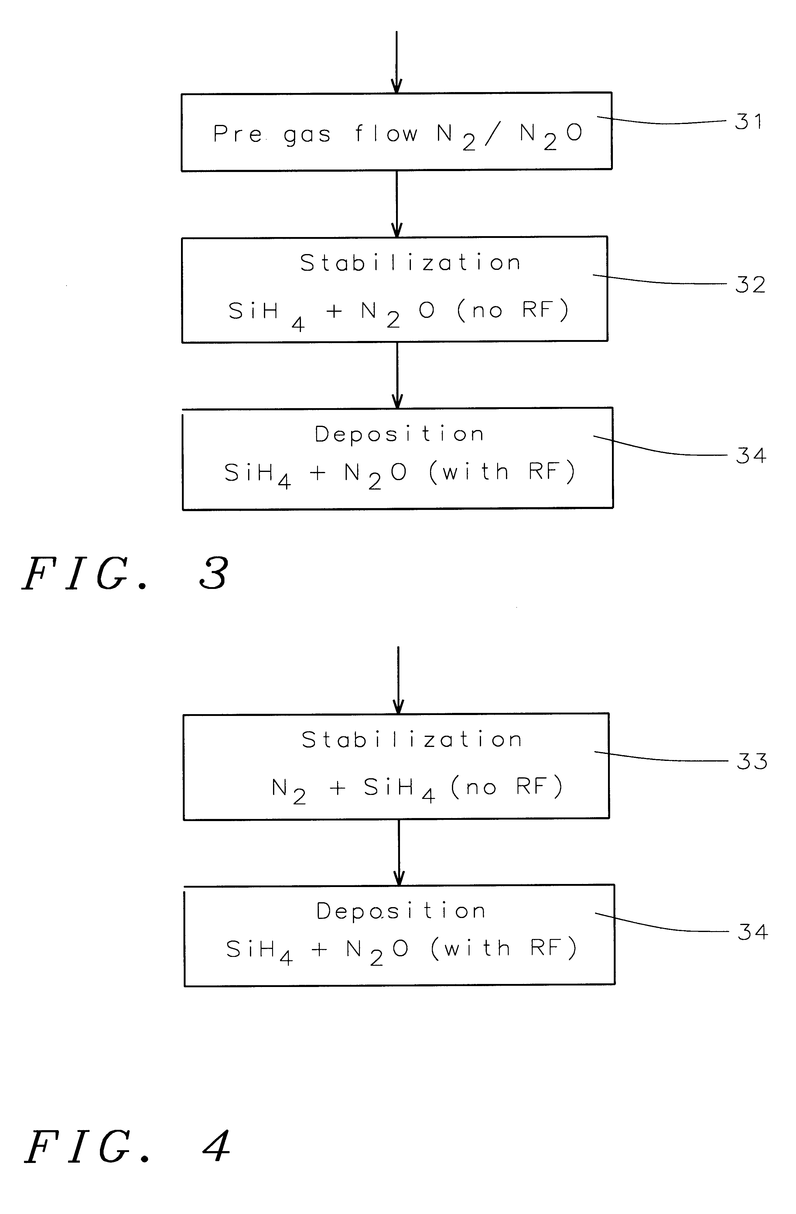
The last table entry (7) refers to the present invention. This is a new stabilization step including N.sub.2 and SiH.sub.4 flow before the N.sub.2 O and SiH.sub.4 deposition step. The particle counts were also satisfactory for this case.

FIG. 4 illustrates the process flow of the second preferred embodiment of the present invention. Step 34 is the conventional deposition step. Step 33 is the new stabilization step of the present invention. N.sub.2 and SiH.sub.4 gases are flowed together in the new stabilization step.

first embodiment

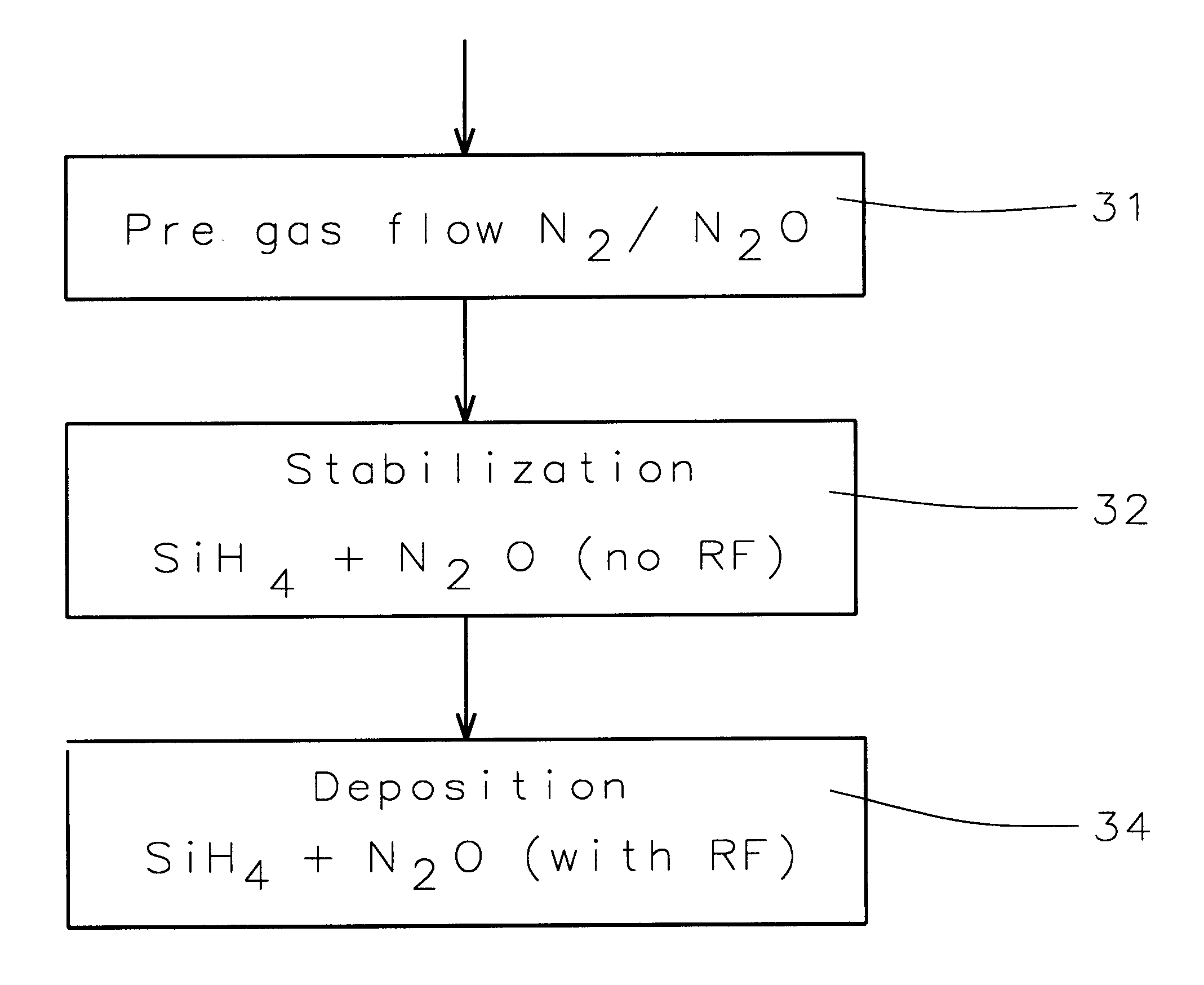
The process of the present invention provides a method of PE-silane oxide deposition with dramatically reduced particle counts. The inventive process in the first embodiment is a pre-flow step inserted before the N.sub.2 O+SiH.sub.4 stabilization step. N.sub.2 O gas or N.sub.2 gas, or a combination of the two, is flowed, preferably for at least 2 seconds. The flow rate of the gases is preferred to be the same as the flow rate of the N.sub.2 O gas in the deposition step.

In an alternative according to the second embodiment, a new stabilization step is inserted in place of the N.sub.2 O+SiH.sub.4 stabilization step. The new step flows N.sub.2 gas and SiH.sub.4 gas using no radio frequency followed by conventional deposition Particle performance was found to be good when this new stabilization step was substituted for the conventional stabilization step. It is surmised that the N2 and SiH4 gases together changed the nucleation conditions.

Both embodiments of the present invention are sim...


PUM

PropertyMeasurementUnit
sizeaaaaaaaaaa
radio frequencyaaaaaaaaaa
purityaaaaaaaaaa

Abstract

A method of forming a PE-silane oxide layer with a greatly reduced particle count is described. A semiconductor substrate is provided over which a silicon oxide film is to be formed. The silicon oxide film is formed by the steps of: 1) pre-flowing a non-silane gas into a deposition chamber for at least two seconds whereby the pre-flowing step prevents formation of particles on the silicon oxide film, and 2) thereafter depositing a silicon oxide film by chemical vapor deposition by flowing a silane gas into the deposition chamber to complete formation of a silicon oxide film using plasma-enhanced chemical vapor deposition in the fabrication of an integrated circuit.

Description

(1) Field of the InventionThe present invention relates to the fabrication of integrated circuit devices, and more particularly, to a method of reducing the number of particles formed on a wafer during PE-silane oxide film formation in the fabrication of integrated circuits.(2) Description of the Prior ArtSilicon oxide films are widely used in semiconductor processing as interlevel and intermetal dielectrics. Silicon oxide films are often formed by plasma-enhanced chemical vapor deposition (PECVD). FIG. 1 illustrates a typical CVD chamber 20. The wafer is placed into the chamber. Gases are flowed into the chamber whereby the silicon oxide film is formed on the surface of the wafer. Typically, silane (SiH.sub.4) is flowed from the Mass Flow Controller (MFC) of one gas inlet 22 while N.sub.2 O is flowed from the MFC of a second gas inlet 24. The reaction of the two gases forms SiO.sub.2.In the typical silicon oxide PE-silane reaction, the SiH.sub.4 and N.sub.2 O gases are flowed into ...

Claims


Application Information

Patent Timeline
Patent Type & Authority Patents(United States)
IPC IPC(8): C23C16/02C23C16/40H01L21/02H01L21/316
CPCC23C16/02C23C16/402H01L21/02164H01L21/31612H01L21/02274H01L21/02312H01L21/02211
Inventor TSAN, CHUN-CHINGCHIEN, HUNG-JUCHEN, CHUN-CHANGWANG, YING-LANG
Owner TAIWAN SEMICON MFG CO LTD
Why Eureka
Try Eureka