Pattern inspection equipment, pattern inspection method, and storage medium storing pattern inspection program

a technology of pattern inspection and equipment, applied in the field of pattern inspection equipment, can solve the problems of poor lsis yield, inspection equipment often determines that the photomask pattern is defective, and the optical image taken from the actual photomask pattern generated on the glass substrate does not correctly match with the design pattern

Inactive Publication Date: 2002-06-04
KK TOSHIBA
View PDF12 Cites 26 Cited by
  • Summary
  • Abstract
  • Description
  • Claims
  • Application Information

AI Technical Summary

Problems solved by technology

The yields of LSIs becomes poor if patterns of the photomasks have faults.
Then, an optical image taken from the actual photomask patterns generated on the glass substrate does not correctly match with designed patterns.
As a result, the pattern inspection equipment frequently determines that the photomask patterns are defective even if they are substantially homothetic transformation of the designed patterns.
And, if designed patterns are used as they are to inspect actual patterns, they will lead to erroneous results determining that the actual patterns have rounded corners and are defective, even if they are substantially same geometry as the designed patterns.
Even if the actual photomask patterns have sharp edges, the measured pattern data does not provide perfect rectangular waveforms because the measured pattern data involves a blur produced by the optical observation system.
As a result, the adjustment of design data to match with actual photomask patterns is restricted by the pixel size, and if a pattern edge is displaced by half a pixel size, the pattern inspection equipment will detect it as a fault.
This, however, may result in overlooking actual faults that must be detected.
This idea, however, increases the quantity of the pattern data and needs highspeed data processing circuits to elongate a processing time and increase inspection costs.
More precisely, if an edge of a pattern image crosses the center of a sensor pixel and covers a half of the sensor pixel, the prior art is unable to determine whether it is "1" or "0".
Namely, the rounding process that is carried out pixel by pixel is incapable of precisely expressing actual photomask patterns.
This leads to overlooking fatal faults that must be detected.
However, making the size of each pixel of the binary data smaller than the size of a sensor pixel increases the quantity of the binary data to raise a problem of needing large-capacity storage devices and high-speed data processing circuits.
This technique is unable to completely cope with the corner roundness of actual photomask patterns because the actual corner roundness is irregular depending on corner sizes and types and etching conditions.
In this way, the pattern inspection equipment of the prior art that compares design data used to delineate patterns on a photomask substrate with measured data taken from the delineated actual photomask patterns is unable to adjust the design data to match with the slightly displaced edges of the actual photomask patterns and the minute roundness of the corners of the photomask patterns.
Making the size of a pixel of the developed pattern data smaller than a sensor pixel size to adjust the pattern data to match with the microscopically displaced edges and rounded corners of the actual photomask patterns increases the quantity of the pattern data to raise a need of high-performance computers and high costs.
The prior art is unable to completely adjust the pattern data to the minute edge displacements and corner roundness of the photomask patterns because they are irregular depending on exposing and etching conditions.

Method used


Image

  • Pattern inspection equipment, pattern inspection method, and storage medium storing pattern inspection program
  • Pattern inspection equipment, pattern inspection method, and storage medium storing pattern inspection program
  • Pattern inspection equipment, pattern inspection method, and storage medium storing pattern inspection program

Examples


first embodiment

Outline of Pattern Inspection Equipment

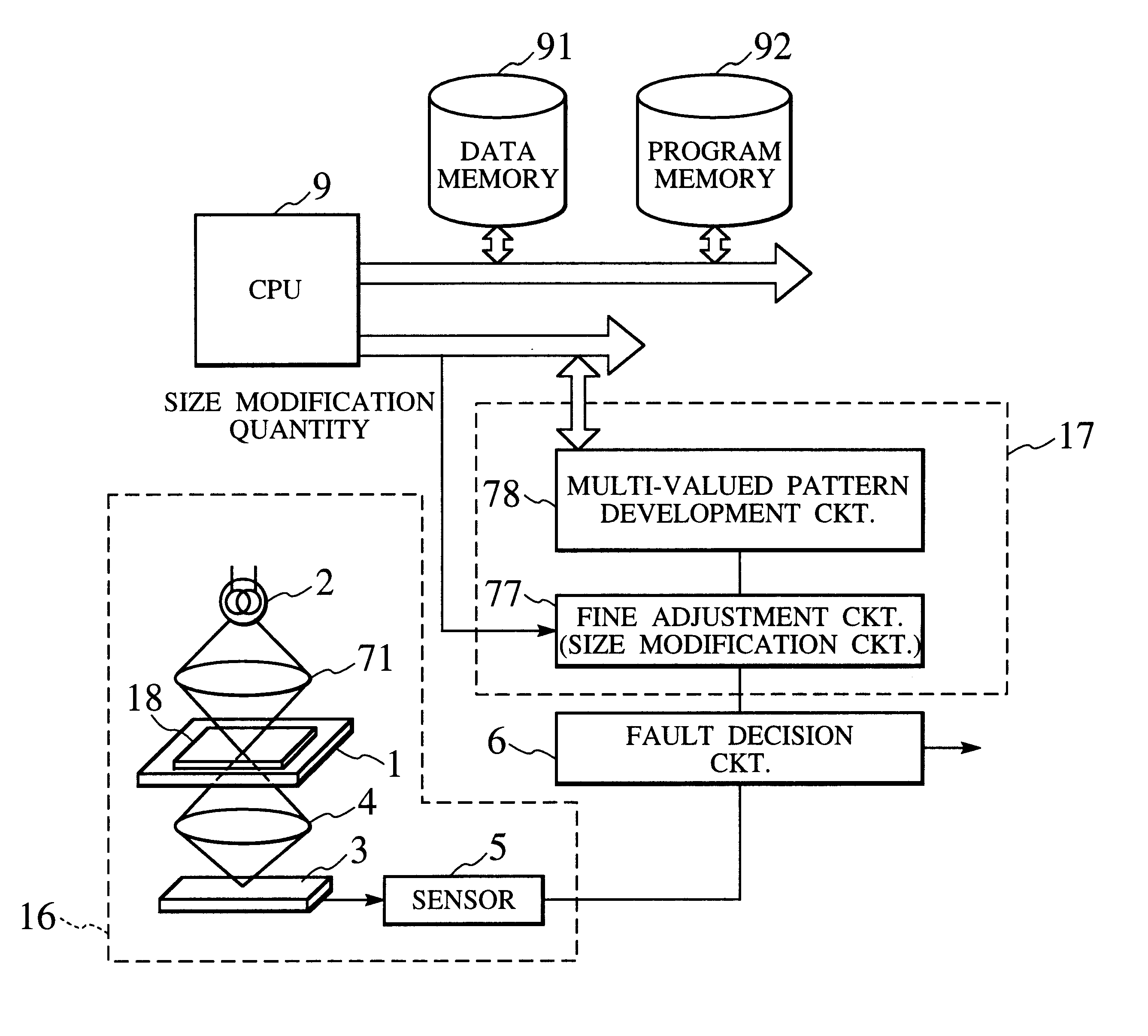
FIG. 3A shows an outline of pattern inspection equipment according to a first embodiment of the present invention. The equipment has at least a measured data generation unit 16 for generating measured data from actual patterns delineated on a sample 1, and a reference data generation unit 17. The equipment also has a host computer having a CPU 9. The CPU 9 has an input unit (not shown) for receiving data and instructions entered by an operator, an output unit (not shown) for providing an inspection result, a data memory 91 for storing design data, and a program memory 92 for storing an inspection program. These elements are connected to one another through a data bus.

The measured data generation unit 16 has an optical image acquiring system including parts 1, 2, 4, and 71, for obtaining an optical image of the patterns, a photoelectric converter 3 for converting the optical image into an analog electric signal, and a sensor circuit 5 for conver...

second embodiment

FIG. 11A shows an outline of pattern inspection equipment according to a second embodiment of the present invention. The equipment has at least a measured data generation unit 16 for generating measured data from actual patterns delineated on a sample 18, and a reference data generation unit 19 for generating reference data used to test if the patterns are sound without faults. The reference data generation unit 19 has a multi-valued pattern development circuit 78 and a fine adjustment circuit 79 connected to the multi-valued pattern development circuit 78. The fine adjustment circuit 79 of the second embodiment differs from that of the first embodiment and is a corner rounding circuit for finely adjusting the roundness of corners in the pattern constructed with the gradational data to match with that of actual pattern. The other arrangements of the second embodiment are substantially the same as those of the first embodiment. Namely, the pattern inspection equipment of the second e...


PUM


Abstract

Pattern inspection equipment has at least a measured data generation unit for generating measured data from patterns that have been delineated on a sample according to design data, a reference data generation unit for generating reference data used to inspect the patterns from gradational data expressed in multiple gradation levels, and a fault decision circuit for comparing the measured data with the reference data. The reference data generation unit has a multi-valued pattern development circuit for developing the design data into the gradational data and a fine adjustment circuit for finely shifting the positions or adjusting the curvatures of pattern edges in the pattern constructed with the gradational data. The fine adjustment of the pattern edges is necessary to cope with slightly displaced edges and rounded corners of the actual patterns on the sample. These slightly displaced edges and rounded corners are caused through mask manufacturing processes and are frequently smaller than the size of a sensor pixel. To adjust the reference data to the displaced edges, a size modification circuit detects a maximum value in a specified area in the gradational data and modifies the size of the pattern constructed with the gradational data. To adjust the reference data to match with the actual rounded corners, a corner rounding circuit rounds corners in the pattern constructed with the gradational data. Also provided is a pattern inspection method for developing the design data into the gradational data, adjusting the gradational data to displaced edges and rounded corners of the actual patterns and preparing the reference data, and testing the patterns for faults. Further provided is a storage medium for storing a pattern inspection program for realizing the pattern inspection method.

Description

1. Field of the InventionThe present invention relates to a technique of inspecting patterns such as photomask patterns formed on a sample used to fabricate semiconductor devices or liquid-crystal display (LCD) devices, or patterns formed on a sample such as a semiconductor or LCD device, to see if the patterns are sound without faults. In particular, the present invention relates to pattern inspection equipment, a pattern inspection method, and a computer-readable storage medium storing a pattern inspection program, for realizing such a technique.2. Description of the Related ArtLarge-scale integrated circuits (LSIs) are manufactured with the use of photolithography and photomasks. The yields of LSIs becomes poor if patterns of the photomasks have faults. Then, various kinds of equipment have been developed to inspect the faults in the photomask patterns.Photomask patterns are formed by depositing a metal film such as a chrome film on a glass substrate, coating the metal film with ...

Claims


Application Information

Patent Timeline
Patent Type & Authority Patents(United States)
IPC IPC(8): G06T7/00
CPCG06T7/0006G06T2207/30148G06T2207/30121
Inventor WATANABE, TOSHIYUKI
Owner KK TOSHIBA
Why Eureka
Try Eureka