Assembly and method for constructing a multi-die integrated circuit

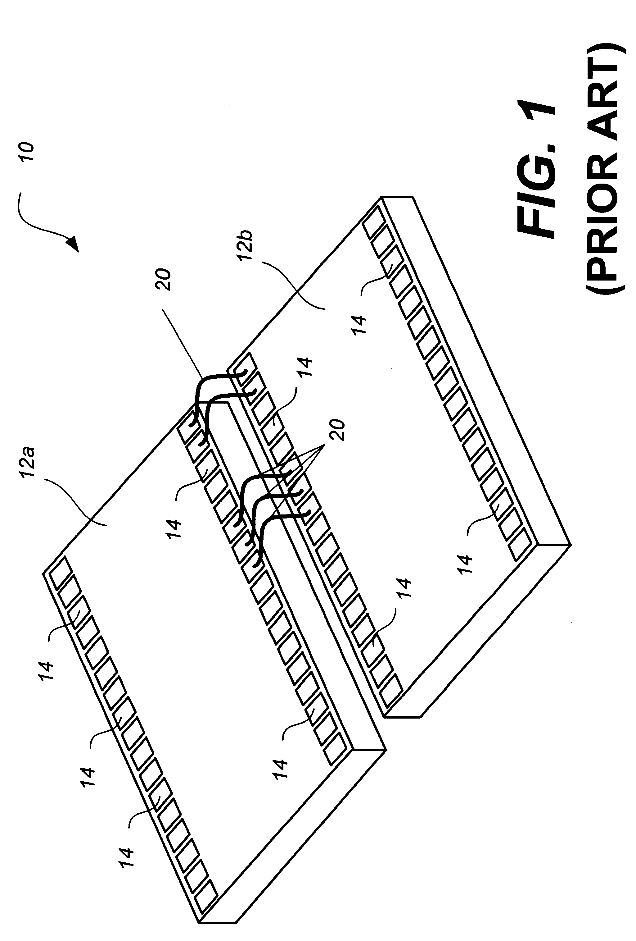
a multi-die, integrated circuit technology, applied in the direction of electrical apparatus construction details, association of printed circuit non-printed electric components, basic electric elements, etc., can solve the problems of high-performance ic products, significant internal routing lengths on a single ic configured on either semiconductor device 12a, 12b, and performance limitation

Inactive Publication Date: 2002-06-11
HEWLETT PACKARD DEV CO LP
View PDF11 Cites 92 Cited by
  • Summary
  • Abstract
  • Description
  • Claims
  • Application Information

AI Technical Summary

Problems solved by technology

As the demand for high speed, high performance, low cost, and portable semiconductor based electronic devices grows the integration density and complexity of semiconductor-packaging technologies continually adapts.
One problem associated with placing multiple semiconductor dies within a single package is related to the distribution of the various signals, which traverse the various semiconductor dies.
At this scale, internal routing lengths on a single IC configured on either semiconductor device 12a, 12b may be significant and performance limiting.
Due to the change in the electrical characteristics (i.e., the characteristic impedance) between internal IC interconnections and the lengthy interface connections, many high-performance IC products (e.g., products having a desired operation at or above a few megahertz) may not meet timing specifications and may be frequency limited.
While the MCM module 10 illustrated in FIG. 1 allows more integrated circuits to be packaged in a single semiconductor package, the MCM 10 stil

Method used


Image

  • Assembly and method for constructing a multi-die integrated circuit
  • Assembly and method for constructing a multi-die integrated circuit
  • Assembly and method for constructing a multi-die integrated circuit

Examples


Embodiment Construction

Having summarized various aspects of the present invention, reference will now be made in detail to the description of the invention as illustrated in the drawings. While the invention will be described in connection with these drawings, there is no intent to limit it to the embodiment or embodiments disclosed therein. On the contrary, the intent is to cover all alternatives, modifications and equivalents included within the spirit and scope of the invention as defined by the appended claims.

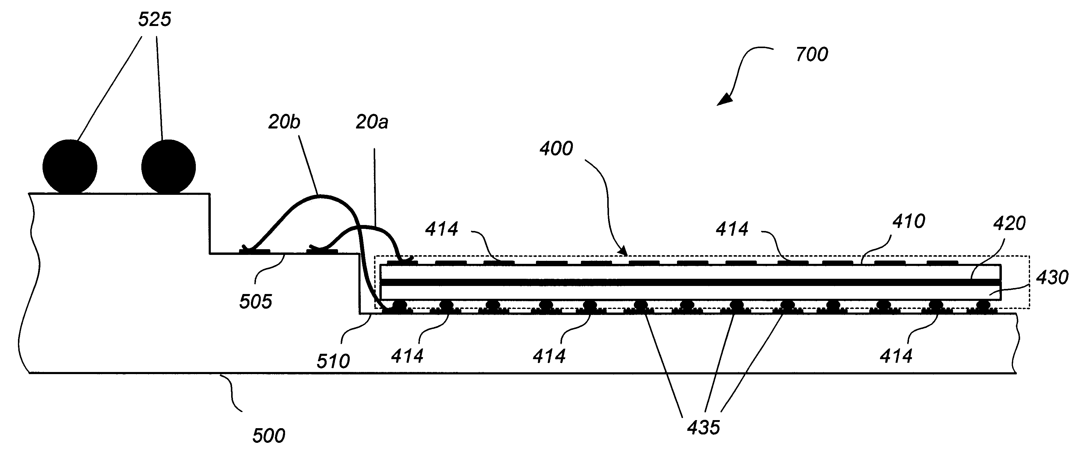
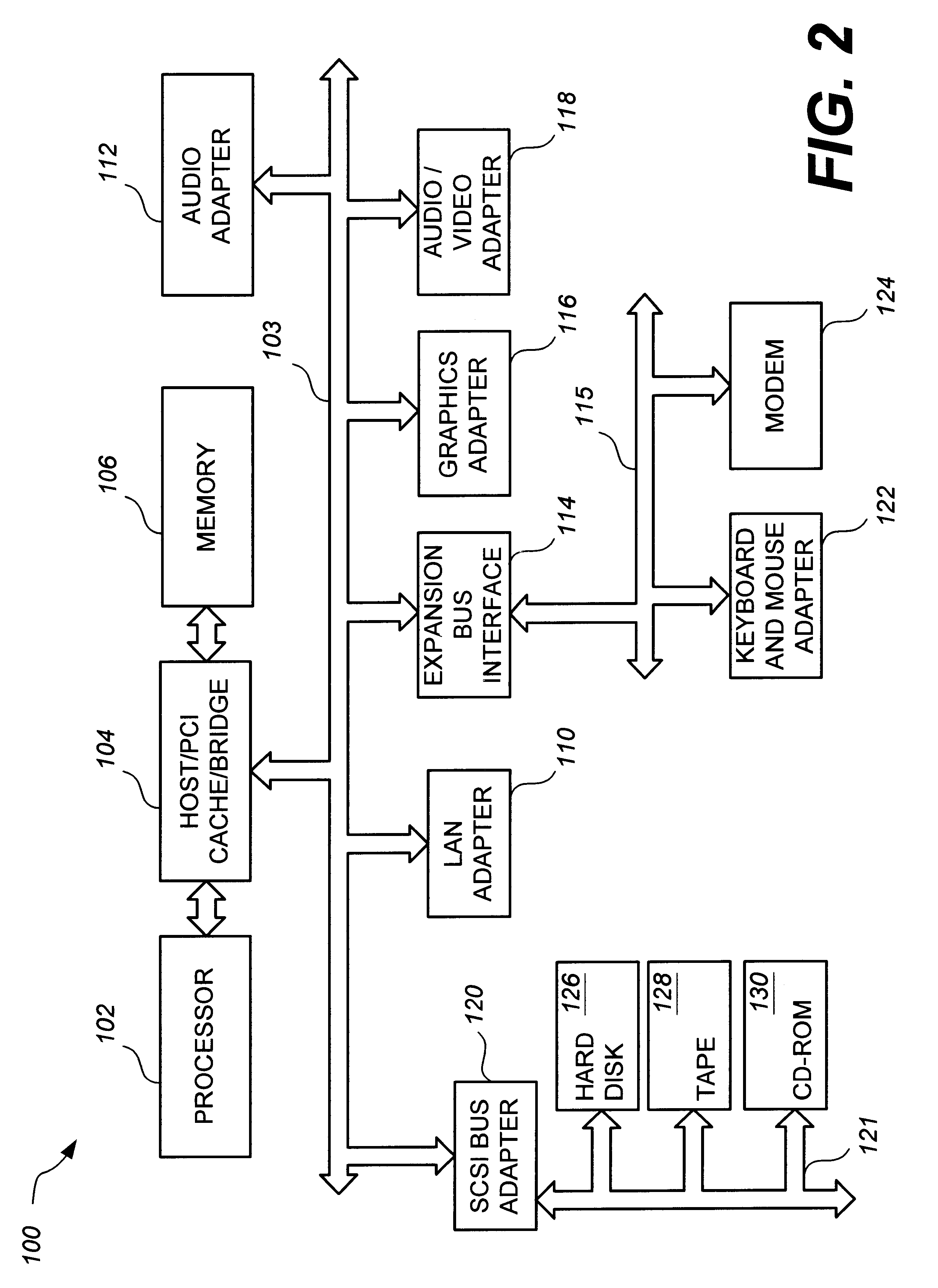
Turning now to the drawings, wherein like reference numerals designate corresponding parts throughout the drawings, reference is made to FIG. 2, which illustrates a schematic of an exemplary operational environment suited for a multi-die IC assembly. In this regard, an exemplary operational environment may comprise a data processing system 100.

As illustrated in FIG. 2, a functional block diagram illustrates the data processing system 100 in which a multi-die integrated circuit assembly may be im...


PUM


Abstract

A multi-die integrated circuit (IC) assembly and method for constructing the same are disclosed. Briefly described, the IC assembly can be constructed with a semiconductor die, a layer of die-attach material, and a flip-chip die. The semiconductor die may contain circuit elements disposed across a top surface of the die. The flip-chip die may be oriented such that circuit elements are disposed across a bottom surface of the flip-chip die. The die-attach material may contact and bond the non-circuit element surfaces of the semiconductor die an the flip-chip die (i.e., the bottom surface of the semiconductor die and the top surface of the flip-chip die). This configuration permits the close arrangements of input/output circuit drivers along the entire perimeter of each of the dies. A method for constructing the multi-die IC assembly is also presented. The method can be broadly summarized by the following steps: arranging a semiconductor die such that circuit components are found on the upper surface of the die; arranging a flip-chip such that circuit components are found on the lower surface of the flip-chip; and introducing a layer of die-attach material such that it contacts and bonds the lower surface of the semiconductor die and the upper surface of the flip-chip.

Description

1. Field of the InventionThe present disclosure relates to semiconductor devices and methods for constructing the same. More particularly, the invention relates to a multi-die integrated circuit (IC) assembly integrating multiple dies.2. Discussion of the Related ArtGenerally, the integrated circuit (IC) industry is continually attempting to improve the frequency of operation, performance, and integration density of integrated circuits (ICs) while simultaneously attempting to add new functionality and features to the same ICs. In order to improve performance while simultaneously increasing functionality, many different fabrication and packaging techniques are being utilized or proposed for use in the industry.A number of different packaging technologies exist for attaching semiconductor devices to a printed circuit board (PCB). Three exemplary packaging technologies include ball-grid array (BGA), chip scale package (CSP), and direct chip attach (DCA). BGA is an older technology rela...

Claims


Application Information

Patent Timeline
IPC IPC(8): H01L25/065
CPCH01L24/49H01L25/0657H01L2924/014H01L2924/01033H01L2924/3011H01L2924/30107H01L2924/19107H01L2924/15321H01L2924/1532H01L2924/15311H01L2924/15165H01L2924/15153H01L2924/1433H01L2924/14H01L2224/16H01L2224/48091H01L2224/48137H01L2224/48227H01L2224/48472H01L2224/49109H01L2224/73265H01L2225/0651H01L2225/06517H01L2225/06572H01L2225/06582H01L2924/00014H01L2924/00H01L2224/05553H01L24/48H01L2224/45099H01L2224/05599
Inventor SLUPE, JAMES P.HARPER, TIMOTHY V.
Owner HEWLETT PACKARD DEV CO LP
Why Eureka
Try Eureka