

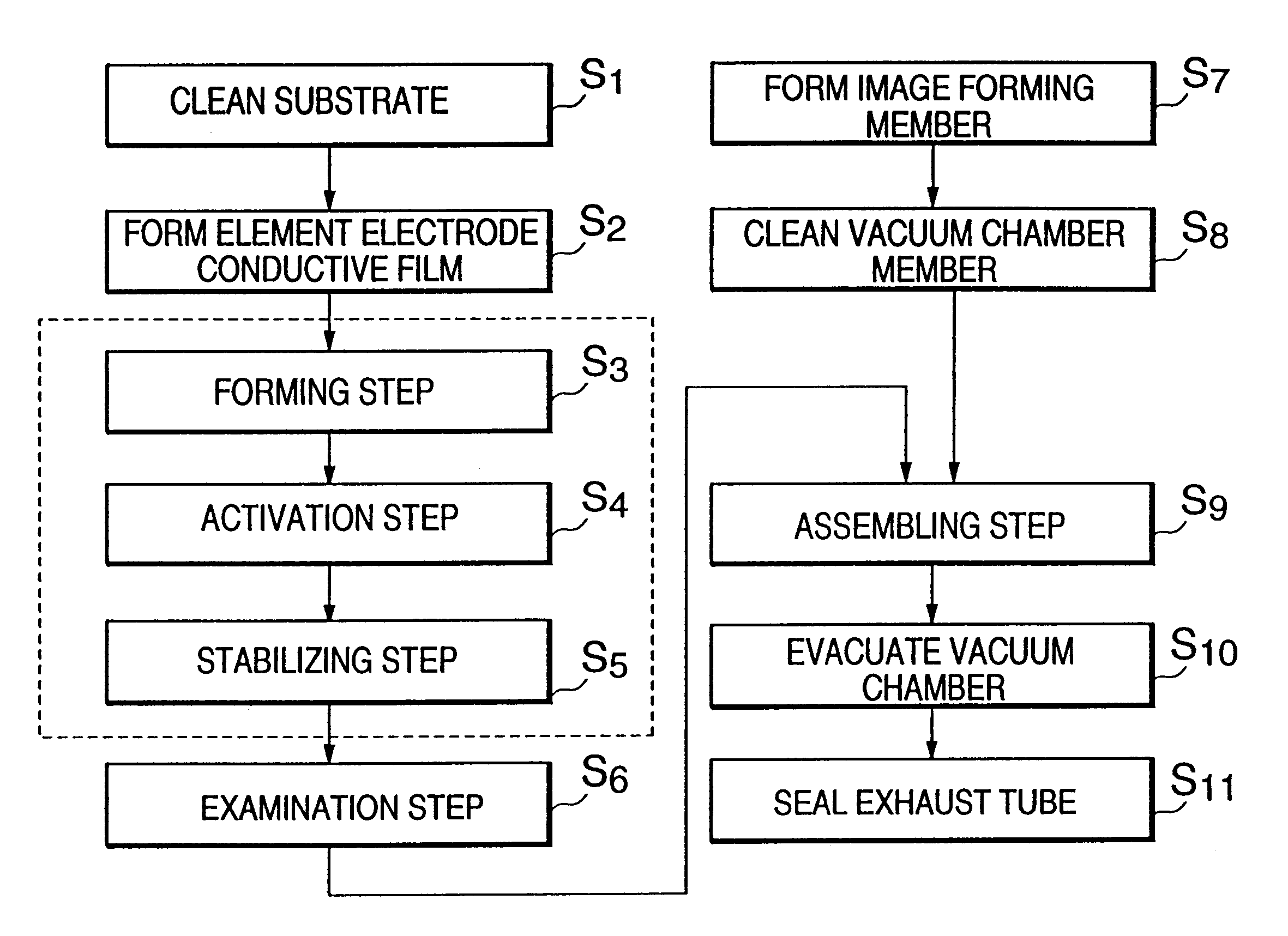
Electron source manufacturing method, and image forming apparatus method
a manufacturing method and electron source technology, applied in the manufacture of sparking plugs, tube/lamp factory adjustment, sparking plugs, etc., can solve the problems of high polymer hardness, difficult to contain dilution gas in a deposit film, and inability to repair
- Summary
- Abstract
- Description
- Claims
- Application Information
AI Technical Summary
Problems solved by technology
Method used
Image

Examples
seventh embodiment
The processes A and B of the seventh embodiment were performed. Next, the following processes were performed.
(Process D)
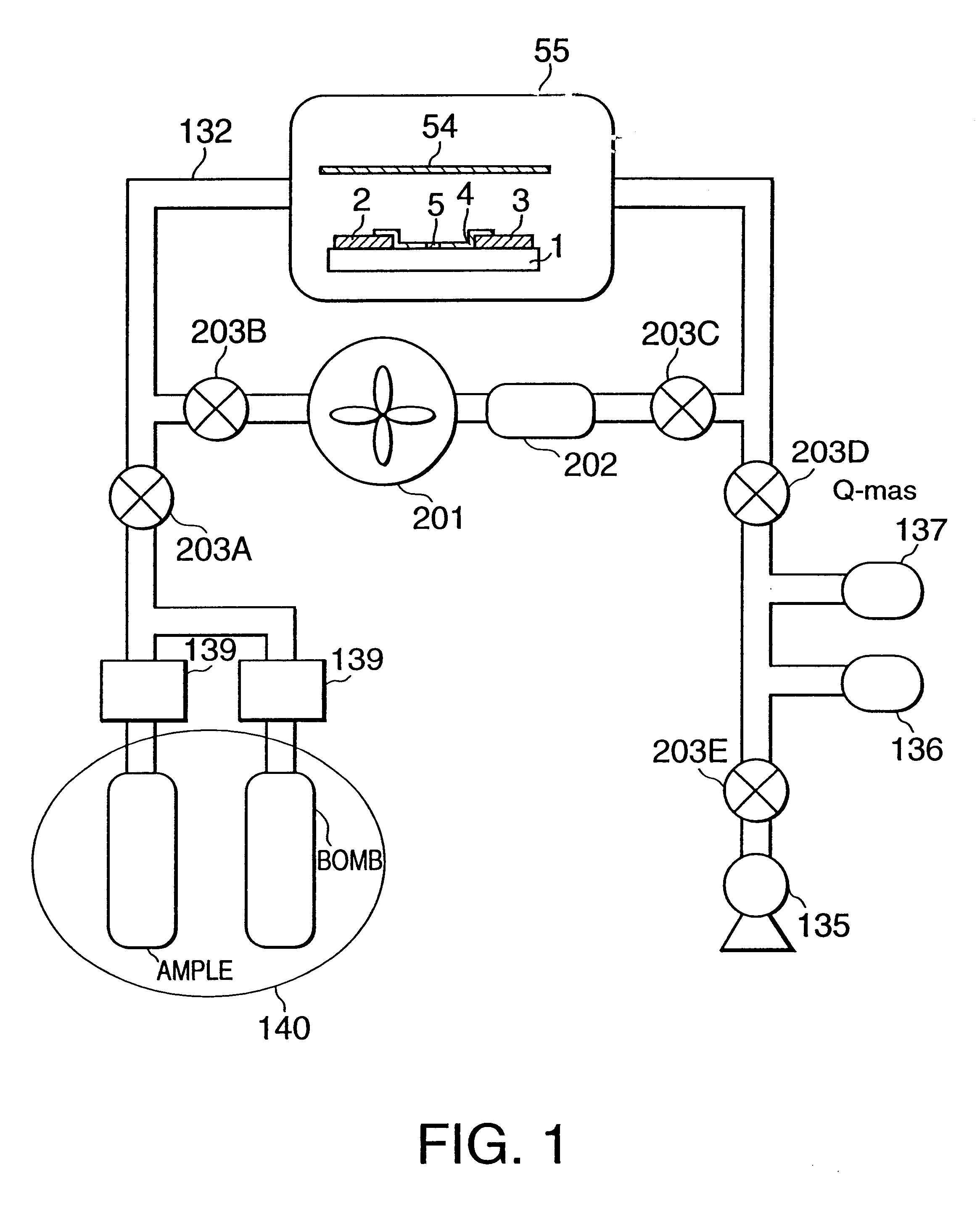
The element was placed in the vacuum process system and the inside thereof was evacuated to 10.sup.-3 Pa or lower. This vacuum process system is not only being capable of evacuating the vacuum chamber but also being capable of introducing proper gas, and has terminals for connecting to the wiring patterns of the element. It took 1 hour and 15 minutes to lower to the above-described pressure.
First, the forming process was performed. Triangular pulses with their peak value being gradually raised such as shown in FIG. 5B were applied across the element electrodes to form the electron emitting area.
(Process E)
Next, the activating process was performed. After the pressure in the vacuum chamber was lowered once to 1.times.10.sup.-6 Pa, acetone was introduced and the pressure was set to 3.times.10.sup.-1 Pa. Then, rectangular pulses of 14 V were applied across the element...
eighth embodiment
The eighth embodiment provides an electron source having a number of surface conduction type electron emitting elements wired in a matrix shape and an image forming apparatus using such an electron source. The manufacture processes will be described with reference to FIGS. 32A to 32E.
(Process A)
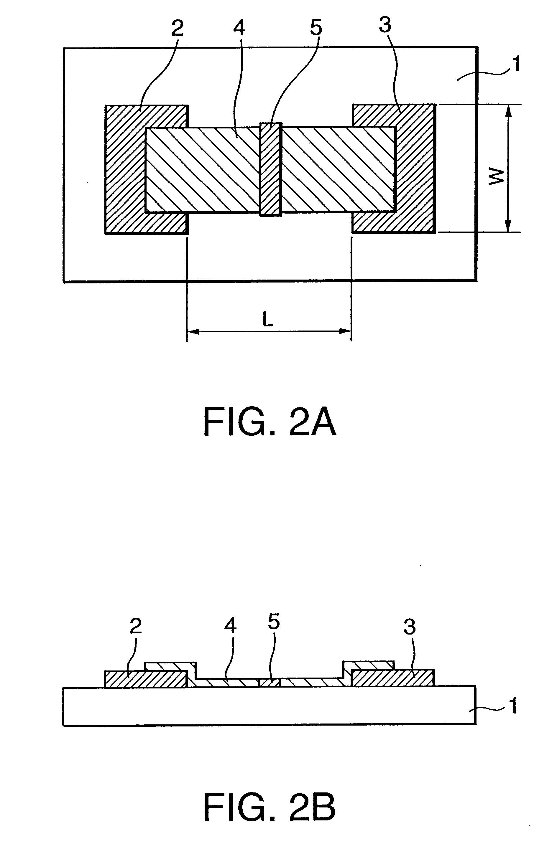
On a cleaned blue plate glass, an SiO.sub.2 layer having a thickness of 0.5 .mu.m was formed through sputtering, and this was used as a substrate 1.
On this substrate, element electrodes 2 and 3 of a surface conduction type electron emitting element were formed through sputtering and photolithography. The material of the element electrodes was a lamination of 5 nm thick Ti and 100 nm thick Ni. The space between element electrodes was set to 2 .mu.m (FIG. 32A).
(Process B)
Next, Ag paste was printed to have a predetermined shape and cured to form Y-direction wiring patterns 91. The width of the wiring pattern was 100 .mu.m and the thickness was about 10 .mu.m (FIG. 32B).
(Process C)
Next, an insula...
ninth embodiment
The ninth embodiment provides an electron source and an image forming apparatus using the electron source, similar to the eighth embodiment. The processes A to E of the eighth embodiment were performed.
(Process F)
The forming process was performed. The electron source was placed in a forming process chamber into which N.sub.2 gas was introduced. The connection is fundamentally the same as that shown in FIG. 33, excepting that a switching device is connected between the pulse generator 3305 and the X-direction wiring patterns to sequentially switch between the X-direction wiring patterns each time one pulse is applied. Rectangular pulses having a peak value of 5 V and a pulse width of 100 .mu.sec were sequentially applied to each X-direction wiring pattern.
Next, the gas introduced into the chamber was changed to a mixture gas of 99% N.sub.2 and 1% H.sub.2.
The resistance of each element increased first very little, then gradually lowered, and thereafter increased abruptly to make a hig...
PUM
 Abstract
Description
Claims
Application Information