Printed wiring board with joining pin and manufacturing method therefor

a printing board and joining pin technology, applied in the direction of electrical apparatus construction details, sustainable manufacturing/processing, final product manufacturing, etc., can solve the problems of difficult to secure a sufficient space and conventional printed wiring boards, and achieve the effect of high density wiring structures

Inactive Publication Date: 2002-09-03
ISHIDA NAOTO +1
View PDF23 Cites 19 Cited by
  • Summary
  • Abstract
  • Description
  • Claims
  • Application Information

AI Technical Summary

Benefits of technology

An operation and effects of the present invention will now be explained.
In the printed wiring board of the present invention, the joining pin is inserted into the through hole. The joining pin has the joining head portion for joining the joining pin to the opposite party pad. Therefore, the through hole and the opposite party pad can be electrically connected to each other by the joining pin by joining the joining head portion to the opposite party pad.
Further, since the through hole and the opposite party pad can be connected to each other by the joining pin in a facing state, as in the conventional case, it is unnecessary to arrange a pad for mounting a soldering ball in addition to the through hole. With this invention, it is also unnecessary to form a conductor circuit for connecting the through hole and the pad for mounting the ball as in the conventional case. Therefore, in the invention a surplus space is formed on a surface of the circuit substrate in a portion except for an opening portion of the through hole. Accordingly, a high density wiring structure can be realized on the substrate surface by forming many other conductor circuits in this space.
The joining pin is manufactured by using a material unmelted at the heating temperature to join the joining pin to the opposite party pad. Therefore, a constant height of the joining head portion is maintained without melting deformation in the above joining. Accordingly, the joining head portion functions as a strut of the printed wiring board at the joining time.
Such a joining head portion functioning as a strut spans a greater diameter than the opening diameter of the through hole. Therefore, when the leg portion of the joining pin is inserted into the through hole, the joining head portion is engaged with the opening portion of the through hole and does not enter the interior of the through hole. Accordingly, the joining head portion can be projected by the same height from a surface of the circuit substrate.
Since no joining pin is melted and deformed at the heating temperature in the joining, it is not necessary to control a melting state of the conductive material for joining. Accordingly, the joining pin and the opposite party pad can be easily joined to each other.

Problems solved by technology

However, the above conventional printed wiring board has the following problems.
Therefore, it is difficult to secure a sufficient space for arranging another conductor circuit on the rear face side of the circuit substrate 96 so that high density wiring is prevented.
Further, since the through hole and the opposite party pad can be connected to each other by the joining pin in a facing state, as in the conventional case, it is unnecessary to arrange a pad for mounting a soldering ball in addition to the through hole.

Method used


Image

  • Printed wiring board with joining pin and manufacturing method therefor
  • Printed wiring board with joining pin and manufacturing method therefor
  • Printed wiring board with joining pin and manufacturing method therefor

Examples


embodiment mode example 1

An example of a printed wiring board in an embodiment mode in the present invention will be explained next by using FIGS. 1 to 10.

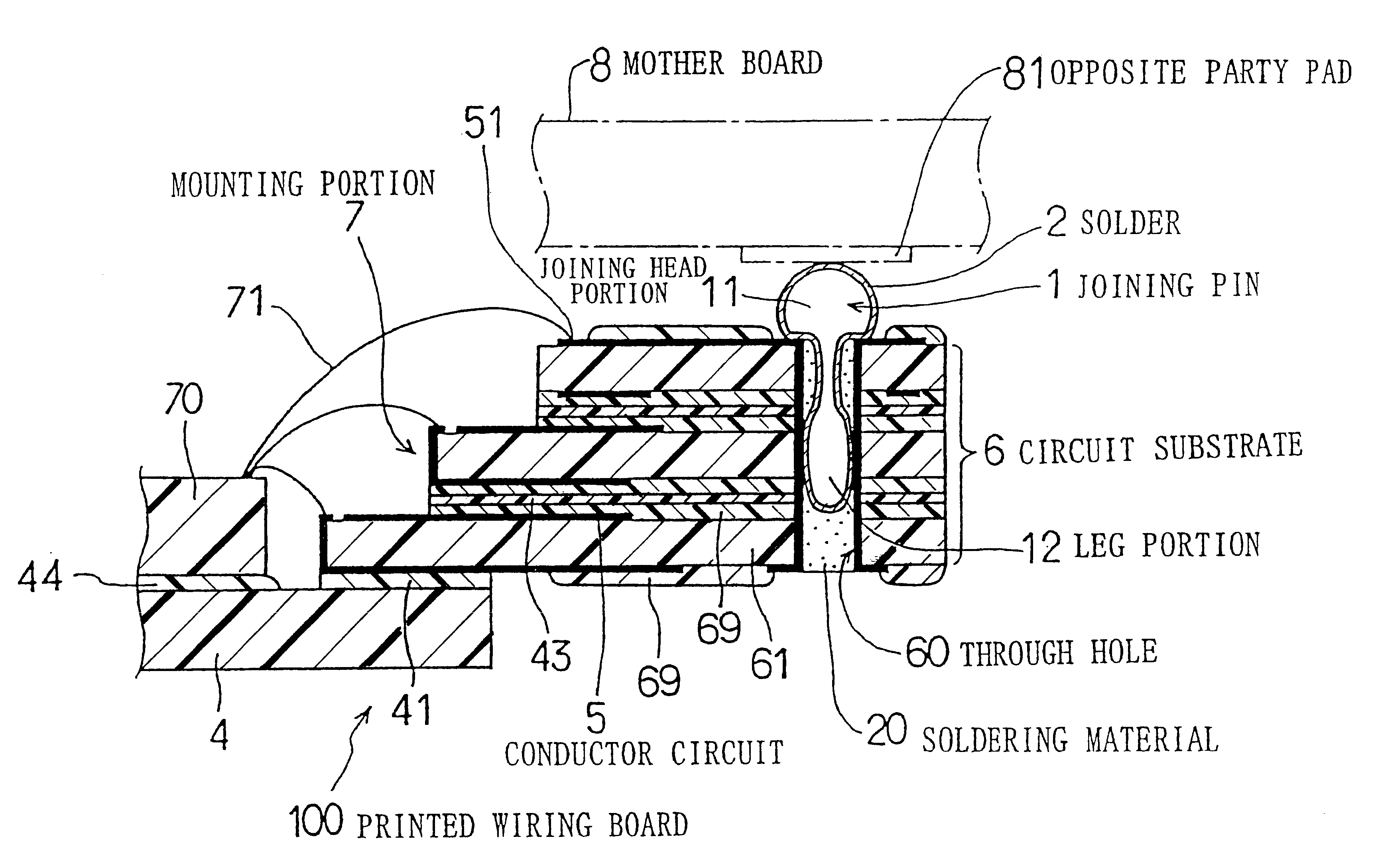
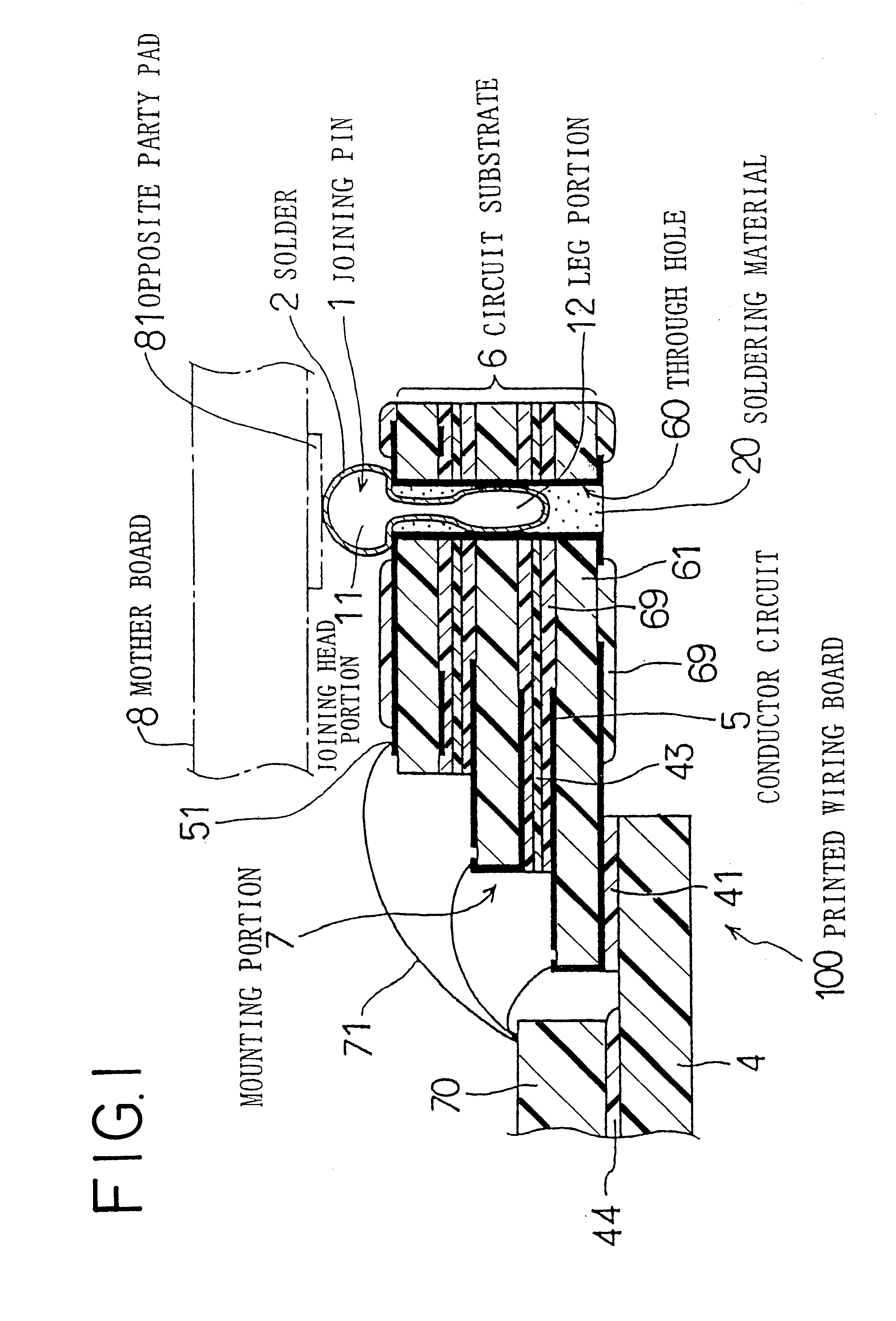
As shown in FIG. 1, the printed wiring board 100 in this example has a circuit substrate 6 having a conductor circuit 5, a through hole 60, and a joining pin 1 inserted into the through hole 60.

The joining pin 1 is manufactured by using a material unmelted at a heating temperature when the joining pin 1 is soldered and joined to an opposite party pad 81 on a mother board 8. For example, the joining pin 1 is manufactured by using covar, phosphor bronze, etc. The joining pin 1 is constructed by an enlarged joining head portion 11 and a leg portion 12. The joining head portion 11 is greater in diameter than an opening diameter of the through hole 60 the leg portion 12. The joining leg portion provides and forms a joining portion for connection to the opposite party pad 81. The joining head portion 11 comprises an enlarged end section which provides an enlarg...

embodiment mode example 2

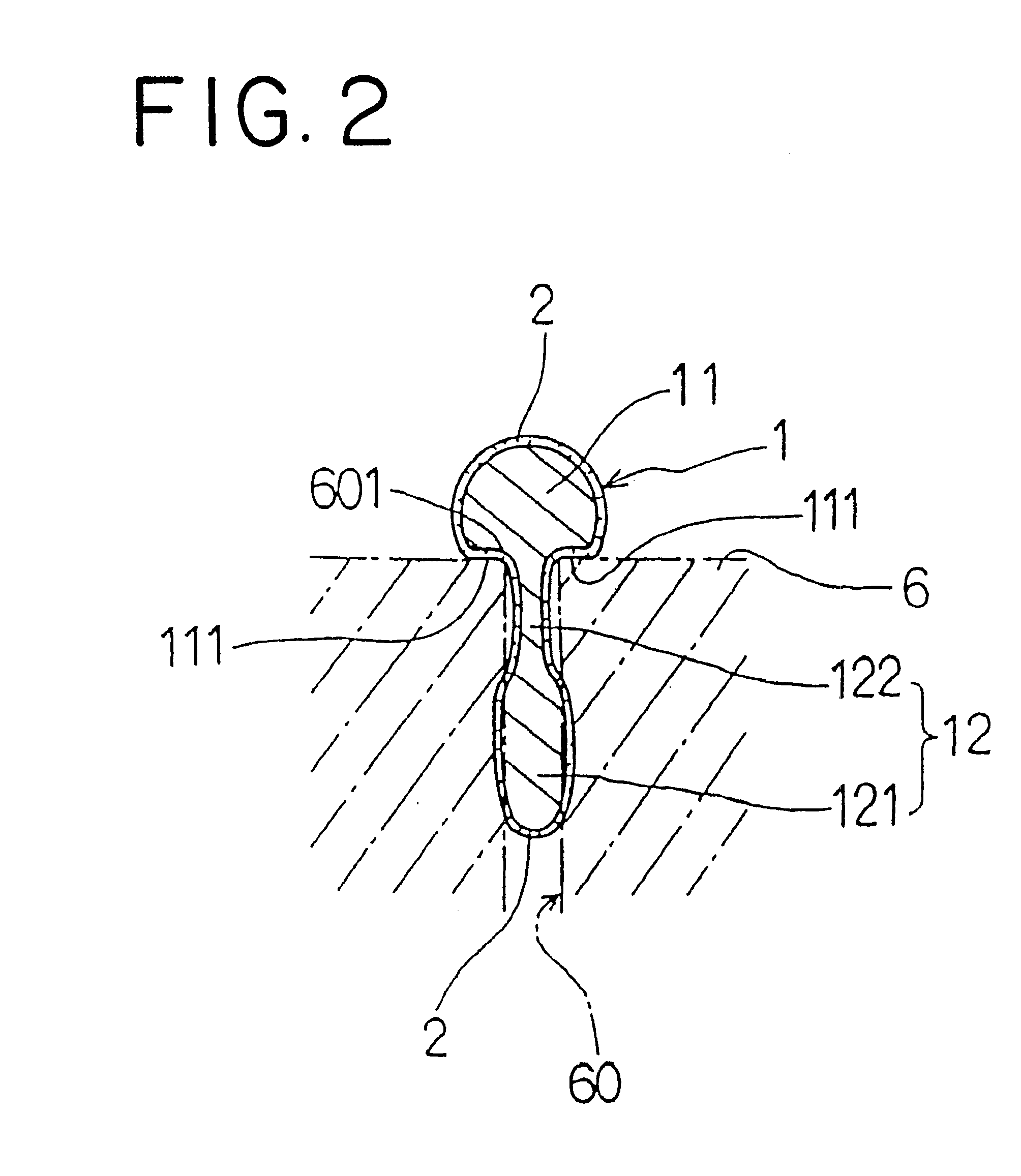
In this example, as shown in FIGS. 11 and 12, a groove 112 for extracting the air is formed in a lower portion 111 of the joining head portion 11 of the joining pin 1.

As shown in FIG. 12, four grooves 112 are formed in a radiating shape from a central portion of the lower portion 111 toward its exterior. Each of the grooves 112 has 0.1 mm in width and 0.05 mm in depth.

A surface of the joining pin in this example is covered with unillustrated solder.

The other constructions are similar to those in the embodiment mode example 1.

In this example, as shown in FIG. 11, when a melted soldering material 20 is flowed into the through hole 60, the air existing within the through hole 60 is discharged outward through a portion between an opening portion 601 of the above through hole 60 and each of the grooves 112. Therefore, no air is sealed within the through hole 60. Accordingly, the entire interior of the through hole 60 can be filled with the soldering material 20 without any clearance.

Effe...

embodiment mode example 3

In this example, as shown in FIGS. 13 and 14, a leg portion 12 of the joining pin 1 has plural projecting portions 125 widened in a radiating shape. Each of the projecting portions 125 has a maximum diameter of 0.35 mm slightly greater than a diameter of the through hole 60.

Similar to the embodiment mode example 2, a groove 112 is formed in a joining head portion 11 of the joining pin 1. As shown in FIGS. 15 and 16, a surface of the joining pin 1 is covered with solder 2. The other constructions are similar to those in the embodiment mode example 1.

In this example, as shown in FIGS. 13 and 14, the plural projecting portions 125 are formed in the leg portion 12 of the joining pin 1. Therefore, as shown in FIGS. 15 and 16, when each projecting portion 125 is inserted into the through hole 60, both ends of the projecting portion 125 are inserted into the through hole 60 while both the ends of the projecting portion 125 locally press against a wall face of the through hole 60, since the...


PUM


Abstract

A printed wiring board has a circuit substrate 6 having a conductor circuit 5 and a through hole 60, and also has a joining pin 1 inserted into the through hole. The joining pin is manufactured by using a material unmelted at a heating temperature in joining the joining pin to an opposite party pad 81. The joining pin is constructed by a joining head portion 11 having a greater diameter than an opening diameter of the through hole. The joining pin forms a joining portion for joining and connection to the opposite party pad. The joining pin has a leg portion 12 having a diameter smaller than the through hole. The leg portion is inserted into the through hole and is joined to the through hole by a conductive material such as a soldering material 20, etc. In lieu of a joining pin, a joining ball approximately having a spherical shape can be joined to the through hole by the conductive material.

Description

1. Technical FieldThe present invention relates to a printed wiring board and its manufacturing method, and particularly relates to joining of the printed wiring board and a mother board.2. Background ArtFor example, as shown in FIG. 27, there is conventionally a printed wiring board having a circuit substrate 96 having a mounting portion 97 for mounting an electronic part 970 thereto, a conductor circuit 95 arranged on a surface of the circuit substrate 96 and also arranged within this circuit substrate 96, and a through hole 93 extending through the circuit substrate 96.The electronic part 970 is electrically connected to the conductor circuit 95 by a bonding wire 971. As shown in FIGS. 27 and 28, a pad 92 for mounting a ball thereto is arranged at an end tip of the conductor circuit 95 on a rear face side of the circuit substrate 96. A soldering ball 91 is joined to a surface of this pad 92.The above conventional printed wiring board 9 is joined to an opposite party pad 981 arran...

Claims


Application Information

Patent Timeline
Patent Type & Authority Patents(United States)
IPC IPC(8): H01L23/48H01L23/498H05K3/34H05K3/36H05K3/30H01L23/12H05K1/11H01R12/00H05K1/14H05K3/46
CPCH05K3/368H05K3/3436H05K3/3426H01L23/49816H01L23/49827H01L23/49833H05K2201/10318H05K2201/10477H01L2224/32245H01L2224/32225H01L24/49H01L24/48H05K2201/10234H05K2201/09481H05K3/308H01L2924/1532H01L2924/15312H01L2924/15173H05K2201/10666H05K2201/10871H01L2224/48091H01L2224/49109H01L2224/73265H01L2924/01077H01L2924/01078H01L2924/01079H01L2924/15153H01L2924/1517H01L2924/00014H01L2224/48227H01L2924/00012H01L2924/00H01L2924/12033H01L24/73H01L2924/14Y02P70/50H01L2224/45099H01L2224/05599H01L2224/85399H01L2224/45015H01L2924/207
Inventor ISHIDA, NAOTOASANO, KOUJI
Owner ISHIDA NAOTO
Why Eureka
Try Eureka