Thermoelectric device

a technology of thermoelectric devices and thermoelectric elements, applied in the direction of thermoelectric device details, basic electric elements, thermoelectric devices, etc., can solve the problems of insufficient solder wetting property, insufficient single-layer nickel plating, and difficult soldering of thermoelectric elements composed of thermoelectric materials

Inactive Publication Date: 2002-09-17
AISIN SEIKI KK
View PDF2 Cites 33 Cited by
  • Summary
  • Abstract
  • Description
  • Claims
  • Application Information

AI Technical Summary

Benefits of technology

According to the present invention, the restraining layer comprises a first layer to prevent the solder ingredient of the solder layer from spreading into the thermoelectric element and a second layer composed of material which has a higher wetting property relative to the solder layer than does the first layer. The first layer is a non-electrolytic plating layer composed of a nickel-phosphorus series, or a non-electrolytic plating layer composed of a nickel series. The second layer has a high wetting property against the solder. The second layer comprised a non-electrolytic plating layer composing of a nickel-boron series. A non-electrolytic plating layer composed of nickel-boron series is slower in the plating speed and more expensive to manufacture than a non-electrolytic plating layer composed of a nickel-phosphorus series. However, nickel-boron has an excellent wetting property relative to the solder when soldering, so that the soldering characteristic of the thermoelectric device is improved.
A non-electrolytic plating layer composed of a nickel-phosphorus series is a little lower in its wetting property, but is faster in the plating speed and cheaper to manufacture than a non-electrolytic plating layer composing of a nickel-boron series.
According to the present invention, the average thickness of the first layer is thicker than that of the second layer to increase the spread prevention effect at low cost since it can be made by a short time process. Though the ratio of the average thickness between the first layer and the second layer is varied by consideration of manufacturing speed or manufacturing cost under usable conditions, it may be set as "the average of the first layer:the average of the second layer=1:(1 to 300)". Preferably, it may be set as "the average of the first layer:the average of the second layer=1:(1 to 100)". More preferably, it may be set as "the average of the first layer:the average of the second layer=1:(2 to 10)". However, the present invention is not so limited.

Problems solved by technology

Furthermore, in general, the thermoelectric element composed of thermoelectric material is hard to solder.
However, a single layer nickel plating is inadequate for combining the characteristics of improved spread prevention and improved soldering.
In other words, if the nickel plating layer is designed for a high level of spread prevention, it can prevent the solder ingredient of the solder layer from spreading the inside of the thermoelectric element, but then it has an insufficient solder wetting property.

Method used


Image

  • Thermoelectric device
  • Thermoelectric device

Examples


embodiment example

Preferred embodiments of the present invention will be described hereinafter in detail with reference to the accompanying drawings.

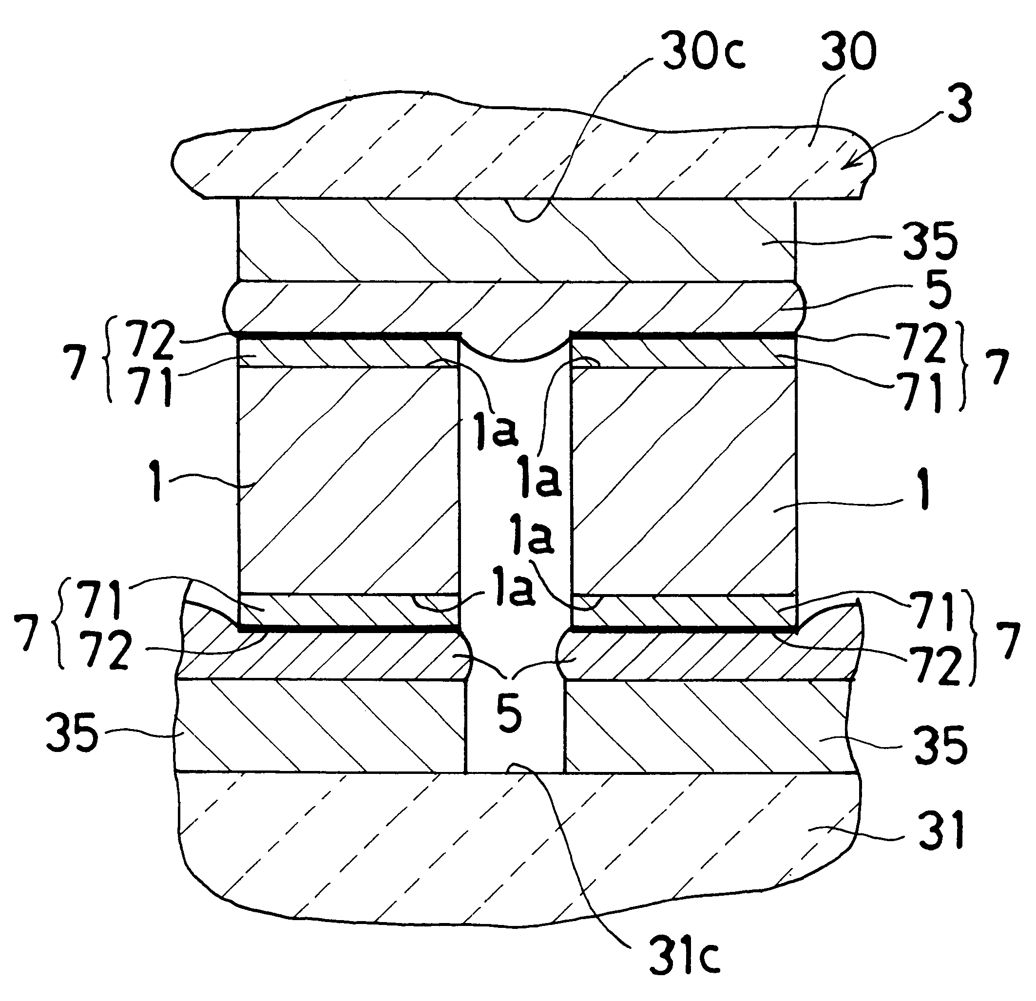
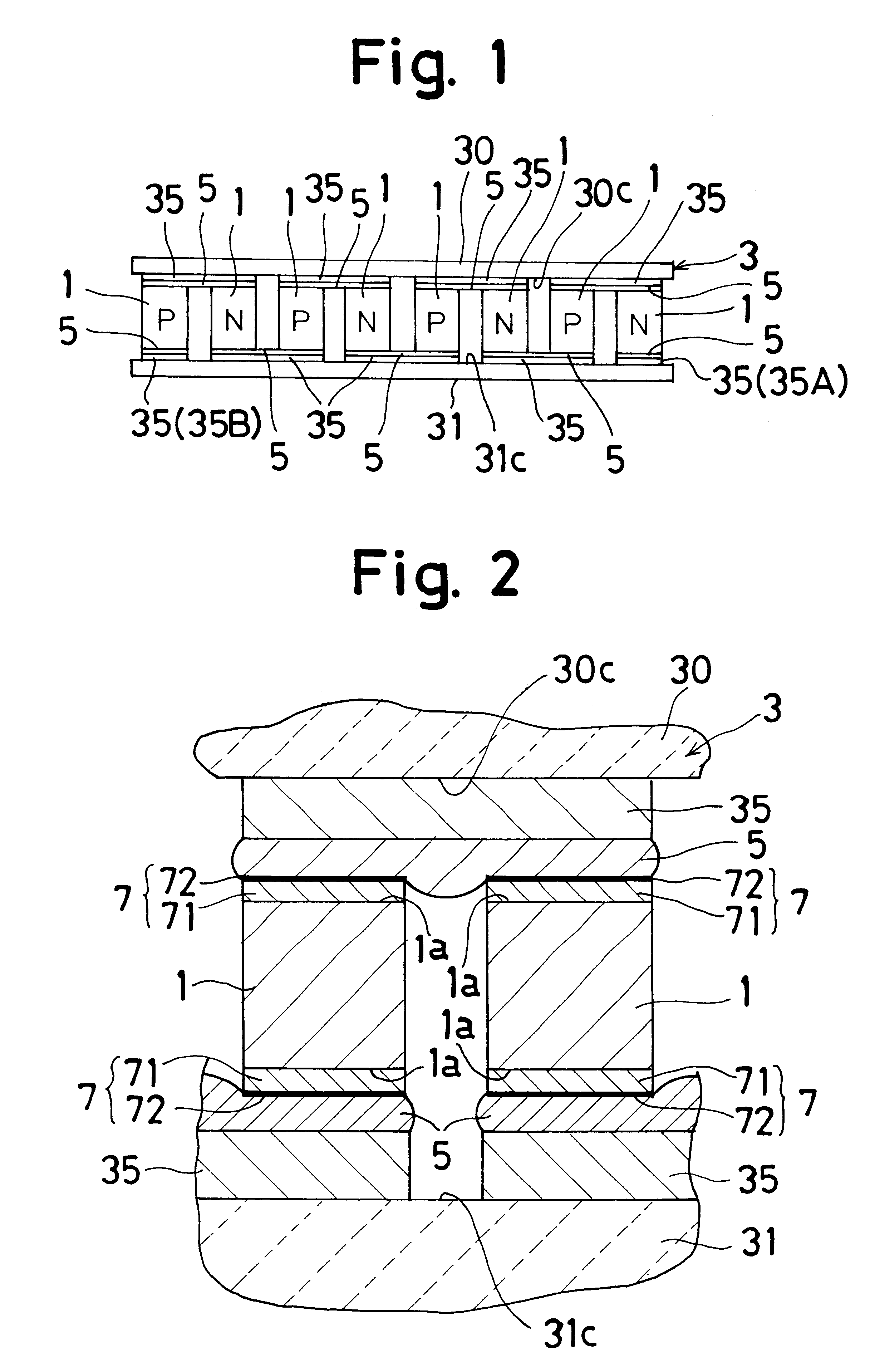
FIG. 1 is a schematic front view of a thermoelectric device according to the embodiment of the present invention. FIG. 2 is schematic cross sectional view of a thermoelectric device according to the embodiment of the present invention. As shown in FIG. 1, the thermoelectric device related to the present invention comprises thermoelectric modules which are made of the thermoelectric element 1, and the counter element 3 countering the element 1. A solder layer 5 adheres the thermoelectric element 1 and the counter element 3 to each other.

The counter element 3 comprises a pair of insulating ceramic substrate (material:alumina) 30, 31 having the planes 30c, 31c for mounting the elements countered each other, and the conductive electrodes (material:copper) 35 lain between said planes 30c, 31c and the solder layer 5. The solder layers 5 are composed of conduct...


PUM

PropertyMeasurementUnit
thicknessaaaaaaaaaa
thicknessaaaaaaaaaa
thicknessaaaaaaaaaa

Abstract

A thermoelectric device includes a thermoelectric element composed of principally thermoelectric material, a counter element adhered to the thermoelectric material. A solder layer lies between the thermoelectric element and the counter element and adheres the thermoelectric element to the counter element. A restraining layer prevents the solder ingredient of the solder layer from spreading into the thermoelectric element. The restraining layer is composed of a first layer to prevent the solder ingredient of the solder layer from spreading into the thermoelectric element and a second layer composed of material having a higher wetting property than the first layer with respect to the solder layer.

Description

1. Field of the InventionThe present invention relates to a thermoelectric device comprising a thermoelectric element composed of principally thermoelectric material.2. Description of the Prior ArtA thermoelectric device comprising a thermoelectric element principally composed of thermoelectric material is well known. The known thermoelectric device has two types of usages, one is as a cooling-heating type device which can cool or heat when electricity is supplied, and the other is as a power generation type which can generate electricity when being cooled or heated.A known conventional thermoelectric device is disclosed in pages 24 to 25 of "Thermoelectric Transfer System Technical General Handbook" published by Realize Company on Jun. 30, 1995 (heisei 7). The nickel plating layer of this device prevents the solder ingredient of the solder layer from spreading into the thermoelectric element, and consists of a single layer. Therefore, the conventional thermoelectric device has adva...

Claims


Application Information

Patent Timeline
Patent Type & Authority Patents(United States)
IPC IPC(8): H01L35/00H01L35/08H01L35/32
CPCH01L35/08H10N10/817
Inventor TAUCHI, HITOSHIOGAWA, SATORUSUGIURA, HIROTSUGUEBINA, NOBURO
Owner AISIN SEIKI KK
Why Eureka
Try Eureka