
Infrared inspection for determining residual films on semiconductor devices

a technology of residual films and infrared inspection, which is applied in the direction of material analysis, optical radiation measurement, instruments, etc., can solve the problems of insufficient sem image, difficult to see residual oxide films and underlying nitride films, and difficult to detect various types of surface anomalies

Inactive Publication Date: 2002-09-17
ADVANCED MICRO DEVICES INC
View PDF14 Cites 36 Cited by
  • Summary
  • Abstract
  • Description
  • Claims
  • Application Information

AI Technical Summary

Problems solved by technology

Various types of surface anomalies have proven difficult to detect using the aforementioned optical, SEM and TEM techniques.
For example, residual oxide films an underlying nitride films have been historically difficult to see using optically microscopy.
The problem stems from the behavior of light reflected from the oxide residue and the underlying nitride film.
While SEM techniques are not prone to the light reflecting issues, structures with irregular topography, such as high aspect ratio trenches, may be not adequately imaged with SEM.
As to TEM imaging techniques, relatively thick films may not be adequately imaged for residue detection purposes.
There are numerous situations in modern semiconductor processing where residual films may adversely impact device performance or yield.

Method used


Image

  • Infrared inspection for determining residual films on semiconductor devices
  • Infrared inspection for determining residual films on semiconductor devices
  • Infrared inspection for determining residual films on semiconductor devices

Examples


Embodiment Construction

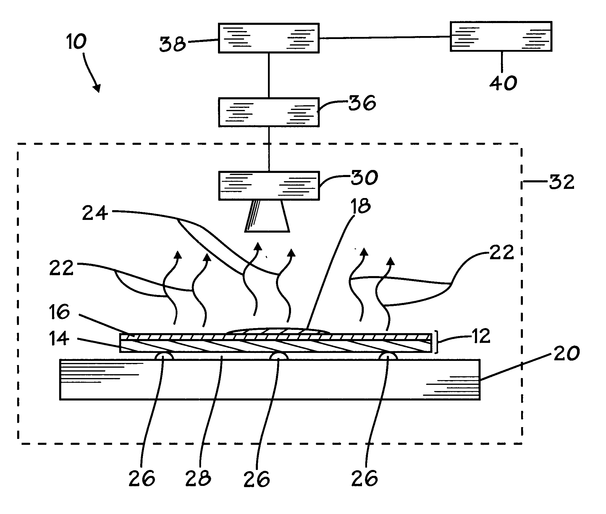
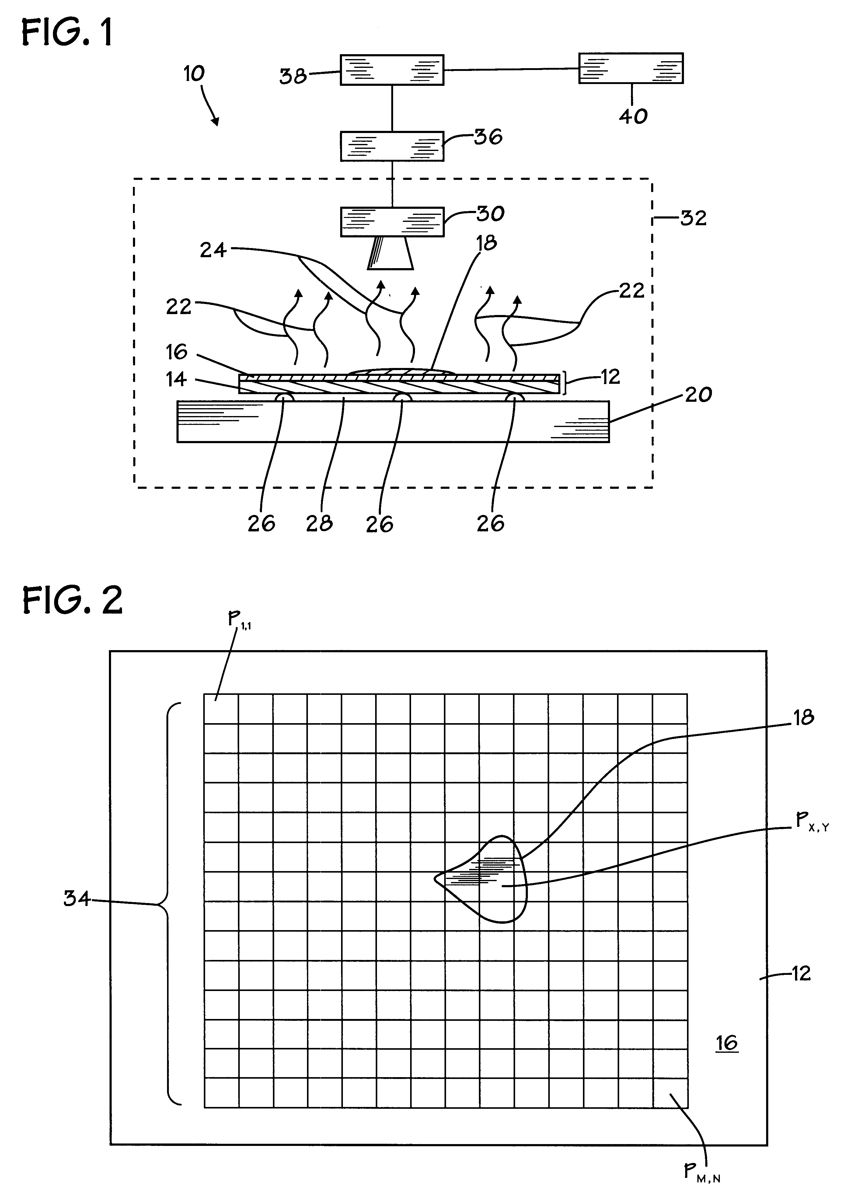
In the drawings described below, reference numerals are generally repeated where identical elements appear in more than one figure. Turning now to the drawings, and in particular to FIG. 1, therein is shown a schematic side view of an exemplary embodiment of an infrared inspection system 10 that is operable to sense and interpret infrared emissions from a semiconductor workpiece 12. In the illustrated embodiment, the workpiece 12 consists of a substrate 14, an overlying film 16 and a residue film 18. The workpiece 12 is seated on a heated stage 20. The stage 20 is brought to an elevated temperature to heat the workpiece 12 to stimulate the emission of infrared radiation 22 from the film 16 and infrared radiation 24 from the residual film 18.

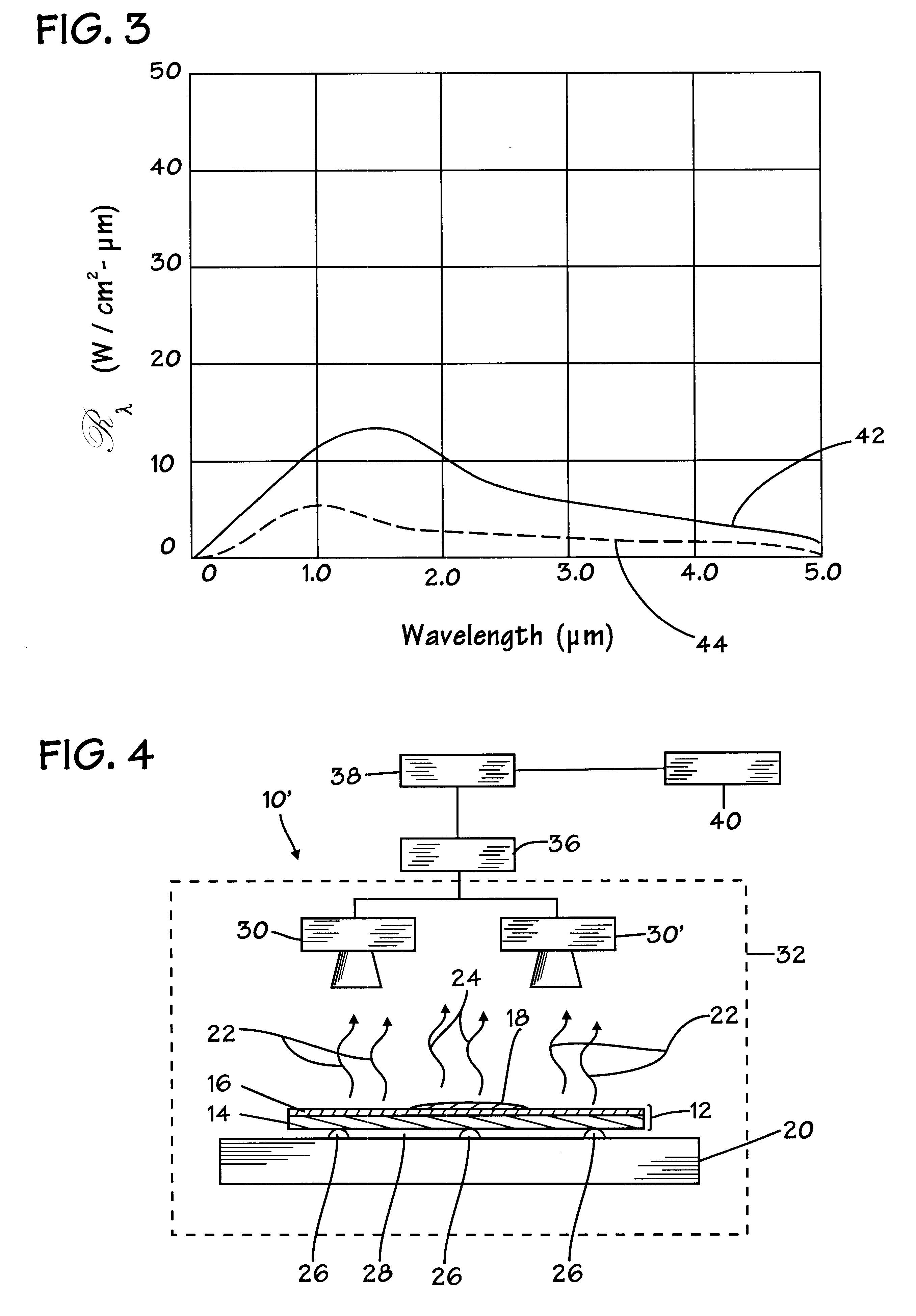
When heated to the same temperature, different solids emit different infrared signatures. As described more fully below, this difference is infrared signatures is used in accordance with the present invention to differentiate unwanted residues fr...


PUM


Abstract

Various methods of inspecting a film on a semiconductor workpiece for a residue are provided. In one aspect, a method of inspecting a film on a semiconductor workpiece wherein the film has a known infrared signature is provided. The method includes heating the workpiece so that the film emits infrared radiation and sensing the infrared radiation emitted from the film. The infrared signature of the radiation emitted from the film is compared with the known infrared signature and a signal indicative of a deviation between the infrared signature of the emitted infrared radiation and the known infrared signature is generated. The method enables the rapid and accurate detection of residues, such as oxide residues on nitride films.

Description

1. Field of the InventionThis invention relates generally to semiconductor processing, and more particularly to a method of inspecting a film on a semiconductor workpiece for residues.2. Description of the Related ArtInspection has been an integral component of semiconductor processing since the development of the earliest germanium-based bipolar integrated circuits. The need for inspection then and now stems from both engineering and economic considerations. Process engineers must be able to track the behavior of the multitude of individual process steps used to fabricate a given integrated circuit. From an economic standpoint, it is critical for semiconductor manufacturers to be able to quickly pinpoint the origin of unacceptable yields so that the circuit design or the fabrication process may be altered as necessary without needlessly wasting lots of wafers that may cost several hundred thousand dollars or more.Morphology of VLSI and ULSI structures is generally determined by thr...

Claims


Application Information

Patent Timeline
IPC IPC(8): G01N21/71
CPCG01N21/71
Inventor NISTLER, JOHN L.RAEDER, CHRISTOPHER H.
Owner ADVANCED MICRO DEVICES INC
Learn More