High speed level shift circuit for low voltage output

a high-speed level and output technology, applied in logic circuit coupling/interface arrangement, pulse technique, semiconductor lasers, etc., can solve the problems of not taking into account power supply variation, required circuit complexity, and significantly increased semiconductor process complexity, etc., to maximise drive capability, minimise voltage headroom, and best efficiency

Inactive Publication Date: 2002-11-19
CIENA
View PDF12 Cites 26 Cited by
  • Summary
  • Abstract
  • Description
  • Claims
  • Application Information

AI Technical Summary

Benefits of technology

Advantageously, level shifting of very high speed logic signals from the positive power rail reference down to a level as close as possible to the ground power rail without use of vertical PNP transistors in the signal path avoids slowing the signal since PNP's are inherently slower than NPN's, and avoids adding considerable complexity of the semiconductor fabrication process that would arise from additional steps required to form vertical PNP's.
Advantageously, signals referenced to the ground rail may be used to drive a very fast long tailed pair output stage with minimal loss of voltage headroom and hence best efficiency.
Advantageously, the present invention maximises the drive capability of such a high speed output signal without invoking any additional power rails or any special process steps in the fabrication of the IC.

Problems solved by technology

Known attempts to level shift very high speed logic signals from a positive power rail reference down to a level as close as possible to a ground or negative rail, however, have encountered a number of problems.
Their use also added considerably to the complexity of the semiconductor process since extra process steps were required in their fabrication.
However this approach did not take account of power supply variation and required circuit complexity to allow for the temperature variation of the forward voltage drop of the diode junction.
Tolerancing these circuits over temperature and power rail variation was therefore difficult since, in general, complexity in the signal path leads to slow circuits.

Method used


Image

  • High speed level shift circuit for low voltage output
  • High speed level shift circuit for low voltage output
  • High speed level shift circuit for low voltage output

Examples


Embodiment Construction

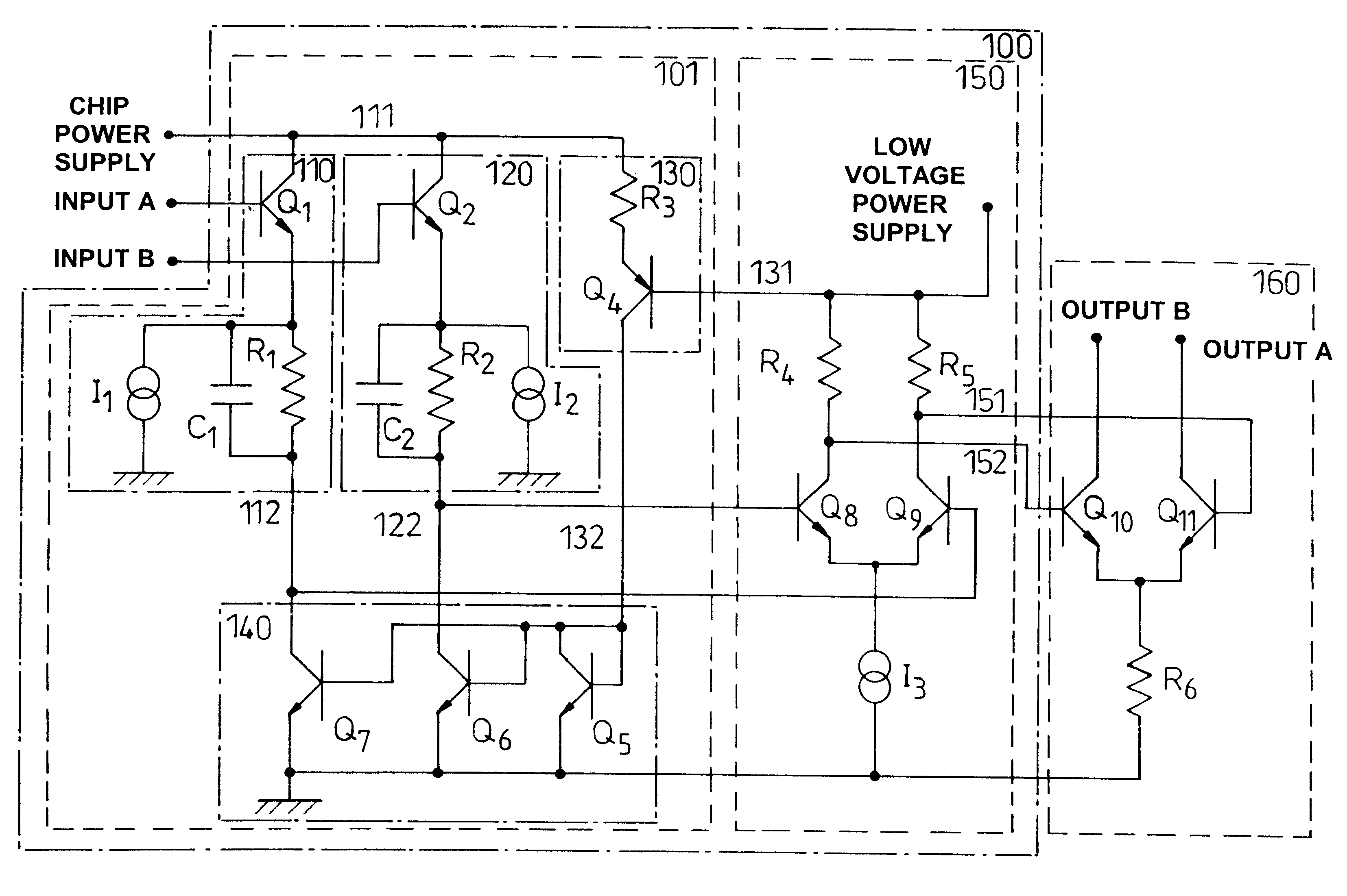
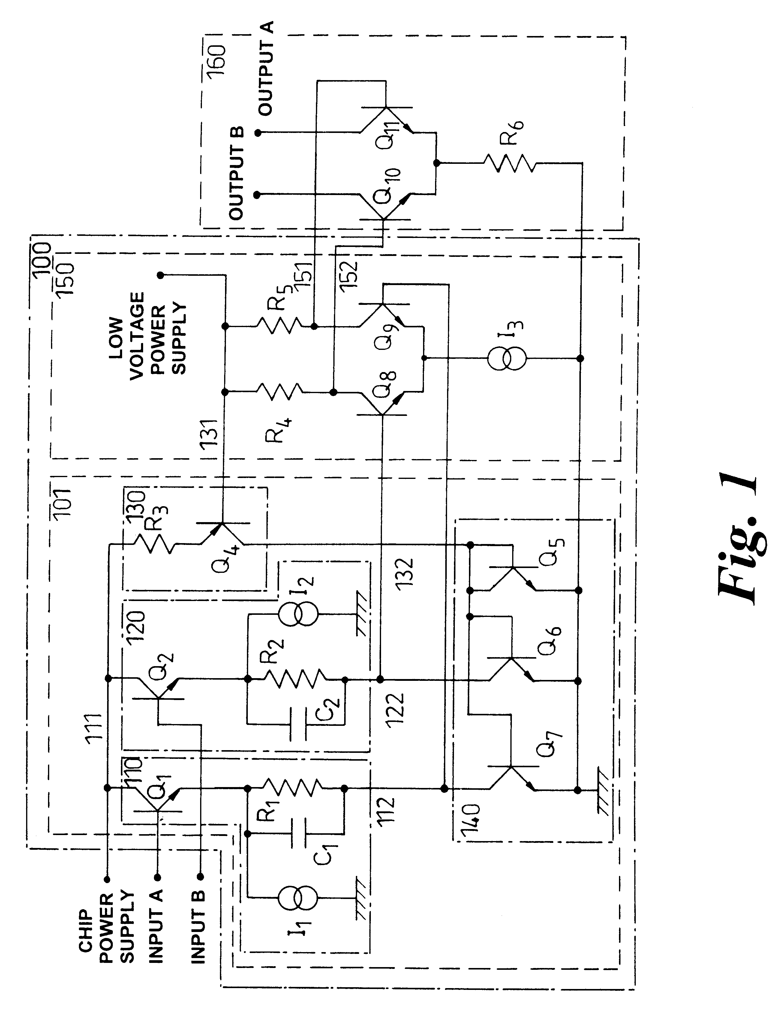
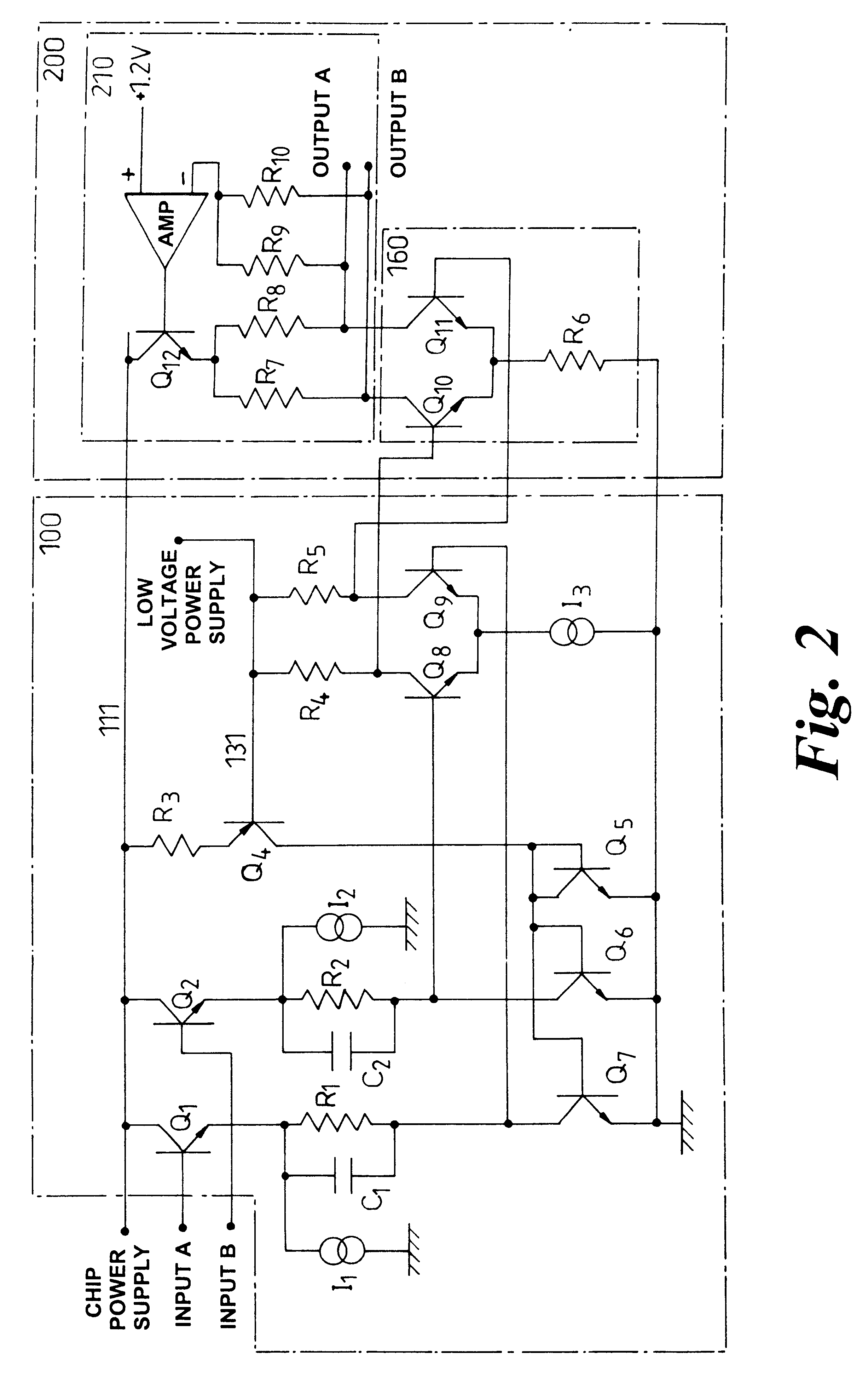
Referring first to FIG. 1, there is shown a first embodiment of a high-speed level shift circuit for low voltage output.

The high speed level shift circuit 100 comprises a re-referencing stage 101 and a regenerating buffer stage 150. In the arrangement shown, the level shift circuit is coupled to an output stage 160.

The re-referencing stage 101 comprises first and second input stages 110, 120, sensing element 130, and current mirror 140.

Input stage 110 comprises a connection to the chip power rail 111 (typically 3.3V.+-.0.3) and a data signal input INPUTA and a signal output 112. It comprises a NPN transistor Q1, resistor R1 capacitor C1, and current source I1. The base connection of Q1 is connected to the data input INPUTA; the collector of Q1 is connected to the chip power rail 111. Resistor R1 is connected in series between the emitter of Q1 and the output port 112. Capacitor C1 is connected in parallel across resistor R1. Current source I1 is connected to the emitter of Q1.

Input ...


PUM


Abstract

An interface circuit from Common Mode Logic to a low voltage, fixed common mode output, with high current drive. The CML signal is received, and then re-referenced to a low-voltage band-gap supply. The circuit is arranged to provide an output data signal referenced to a second positive reference voltage supply responsive to receipt of a common mode input data signal referenced to a first positive reference voltage supply. The circuit avoids use of vertical PNP transistors in the signal path.

Description

The present invention relates to a method and apparatus for high speed level shifting to provide a low voltage output, and a system incorporating the same.BACKGROUND TO THE INVENTIONLogic signals at very high speed are often processed using bipolar Current Mode Logic (CML)--a signalling system involving small voltage swings (typically 250 mV) referenced to the positive supply of the integrated circuit (IC). Output interface levels from an IC using this logic are generally specified with a greater signal swing than 250 mV.For a bipolar transistor to operate at speed it is necessary that its collector base junction does not enter forward conduction. Therefore, in order to allow increased signal swing on the output stage, the logic signals which drive it have to be level shifted from the positive rail reference down to a lower voltage. The more the signal can be shifted the greater the potential output swing.Known attempts to level shift very high speed logic signals from a positive po...

Claims


Application Information

Patent Timeline
Patent Type & Authority Patents(United States)
IPC IPC(8): H03K19/018H01S5/042H01S5/00
CPCH03K19/01831H01S5/042H01S5/0427H01S5/0428
Inventor WHITTAKER, EDWARD JSHERAZI, IMRAN
Owner CIENA
Why Eureka
Try Eureka