Method for operating nonvolatile memory cells

a nonvolatile, memory cell technology, applied in static storage, digital storage, instruments, etc., can solve the problems of undesirable magnitude disparity between the required negative and positive voltages, voltage stress concentrated on one of the cell dielectrics, and the inability to achieve the desired effect of advanced technology,

Inactive Publication Date: 2002-12-10
WINBOND ELECTRONICS CORP
View PDF10 Cites 55 Cited by
  • Summary
  • Abstract
  • Description
  • Claims
  • Application Information

AI Technical Summary

Problems solved by technology

As addressed below, the resulting "magnitude disparity" between the required negative and positive voltages is not a favorable condition for advanced technologies.
More specifically, the magnitude disparity results in voltage stresses concentrated on one of the cell dielectrics.
In this case, the magnitude disparity between the negative and positive voltages becomes very undesirable for three reasons: (1) voltage pumping from a low level (e.g., 3.3 V) supply-voltage is more difficult than from the "old 5 V standard" power supply; (2) the voltage pumping is now likely limited by the breakdown voltages of the available on-chip transistors, especially when transistors become smaller; and (3) because the memory cell size becomes smaller, the associated array decoders must also be small in order to fit into the cell-pitch, which makes high voltage decoding operation difficult or unworkable.

Method used


Image

  • Method for operating nonvolatile memory cells
  • Method for operating nonvolatile memory cells
  • Method for operating nonvolatile memory cells

Examples


Embodiment Construction

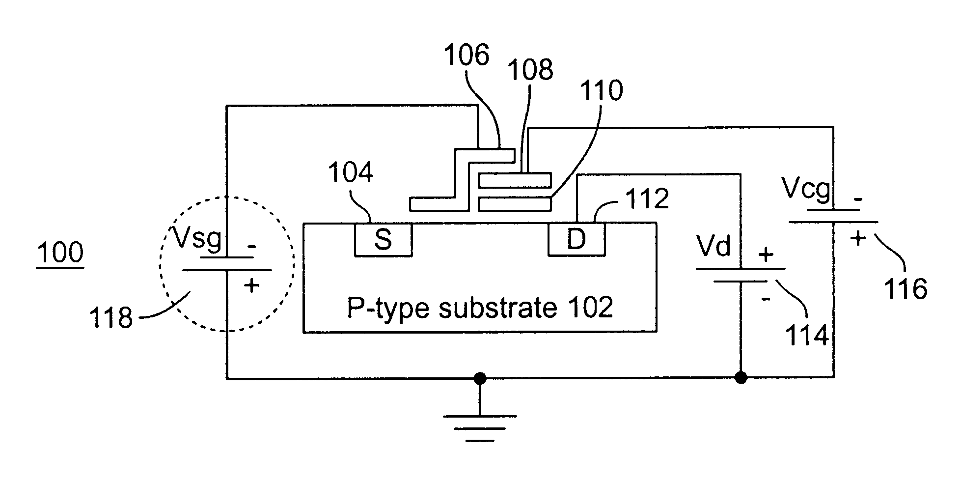
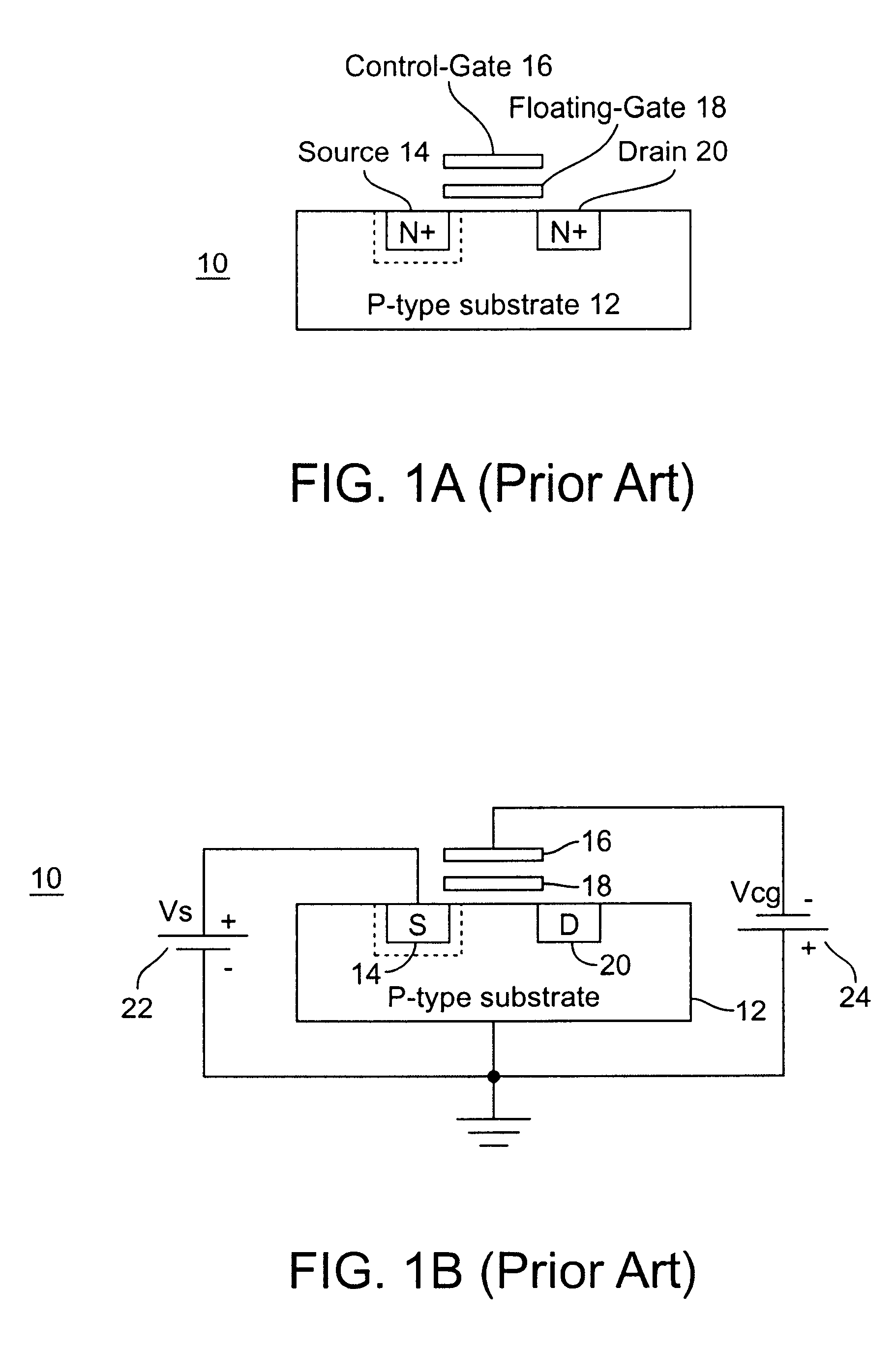
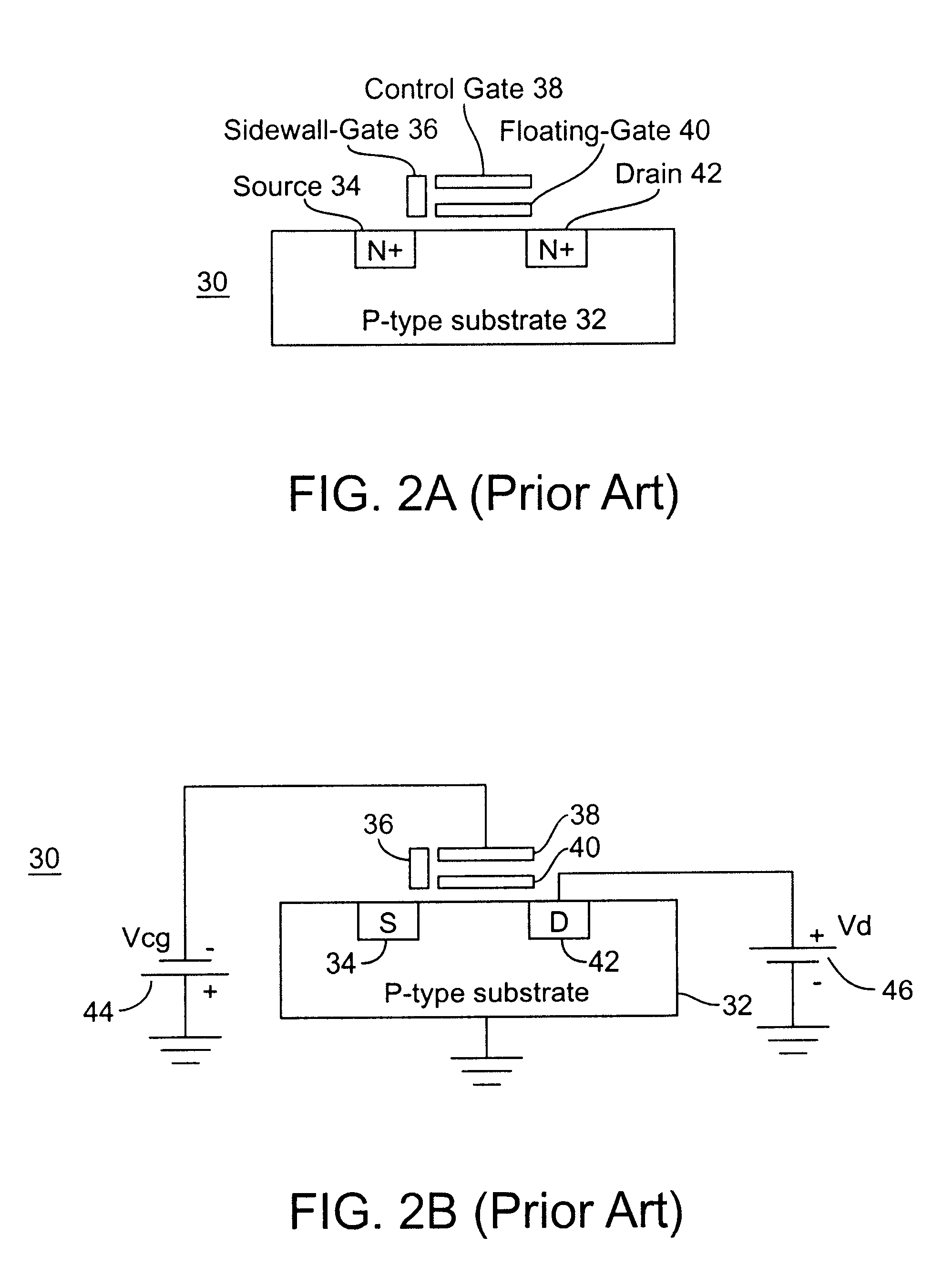
The present invention will be first described within the context of a generic five-terminal flash memory cell. As will become clear in the following description, this invention is applicable to all five-terminal source-side injection memory cell structures, including examples as those shown in FIGS. 2 and 3. A new memory cell structure having an isolatable cell body terminal will be described, as well as the operation advantages of this cell as compared to the conventional cell structure. This particular feature of the invention is applicable to both four-terminal and five-terminal flash memory cells, as will be explained below. While the invention will be described in conjunction with the preferred embodiments, it will be understood that they are not intended to limit the invention to those embodiments. On the contrary, the invention is intended to cover alternatives, modifications and equivalents, which may be included within the spirit and scope of the invention as defined by the...


PUM


Abstract

The present invention is directed at a new nonvolatile memory cell structure, and a new erase method and apparatus for operating this and other nonvolatile memory cells, with special emphasis on source-side injection flash EEPROM cells, which enhances the erase efficiency of the cell. By activating the select-gate terminal of the cell using a negative voltage, it has been found for the first time that the erase performance can be improved. In one preferred embodiment, the present invention provides for three overlapping voltage signals applied to the cell terminals, of which two are negative and one positive. In another preferred embodiment, the memory cell is built on an "internal P-well" within an isolating N-well on the P-type substrate. In this case, by shifting the memory cell's body potential, the erase-mode uses four overlapping erase signals, two of which are negative, and two positive. With experimental data, it is demonstrated that better "magnitude balance" has been achieved for the highest erase voltages of opposite polarities. Since only moderate voltages are needed for the erase operation while maintaining the erase speed, the otherwise stringent requirement on transistor breakdown voltages for on-chip charge pumps and driver circuitry can be relaxed.

Description

1. Field of the InventionThe present invention relates to non-volatile semiconductor memory devices and methods for operating such devices; and more particularly the present invention addresses the method and conditions of erasing nonvolatile memory cells, with special emphasis on triple-polysilicon source-side injection flash EEPROM (electrically erasable and programmable read-only-memory) cells.2. Description of Related ArtA flash memory cell relies on a floating-gate to store electrical charges. The amount and the polarity of these charges affect the ability of the underlying channel to conduct electrical current. Flash memory cells as known today are constructed either in the form of a four-terminal device (with drain, control-gate, source, and substrate), which is typically made using a double-polysilicon process; or in the form of a five-terminal device (with drain, control-gate, select-gate, source, and substrate), which is typically made using a triple-polysilicon process. I...

Claims


Application Information

Patent Timeline
Patent Type & Authority Patents(United States)
IPC IPC(8): G11C16/06G11C16/04G11C16/14
CPCG11C16/0425G11C16/14H10B69/00
Inventor WALD, KEITH R.PANG, CHAN-SUIMA, YUEH YALE
Owner WINBOND ELECTRONICS CORP
Why Eureka
Try Eureka